Junction Profile Engineering Using Staged Thermal Annealing

a junction profile and staged thermal annealing technology, applied in the direction of semiconductor devices, electrical apparatus, transistors, etc., can solve the problems of implanted diffusion, defect generation, and destruction of lattice structures in the source and drain regions, and achieve reduced diffusion, increased activation rate, and high throughput

Inactive Publication Date: 2010-08-19
TAIWAN SEMICON MFG CO LTD
View PDF7 Cites 21 Cited by
  • Summary
  • Abstract
  • Description
  • Claims
  • Application Information

AI Technical Summary

Benefits of technology

[0008]The advantageous features of the present invention include increased activation rate, reduced diffusion, and high throughput in the annealing.

Problems solved by technology

Second, the implantation causes the destruction of the lattice structures in the source and drain regions and hence defects are generated.
However, the RTA, also due to its relatively long time, causes the diffusion of the implanted ions.
This causes the difficulty in the short-channel control.
The problem becomes even more severe with the increasing down-scaling of integrated circuits, which causes the channel regions of the MOS devices to be increasingly shorter, and hence the diffuse length becomes an increasingly greater portion of the channel length.
Unfortunately, the results of all these annealing temperatures and durations, when combined, may enhance or degrade each other.

Method used


Image

  • Junction Profile Engineering Using Staged Thermal Annealing
  • Junction Profile Engineering Using Staged Thermal Annealing
  • Junction Profile Engineering Using Staged Thermal Annealing

Examples


Embodiment Construction

[0015]The making and using of the illustrative embodiments are discussed in detail below. It should be appreciated, however, that the illustrative embodiments provide many applicable inventive concepts that can be embodied in a wide variety of specific contexts. The specific embodiments discussed are merely illustrative of specific ways to make and use the invention and do not limit the scope of the invention.

[0016]A novel method for forming and annealing a metal-oxide-semiconductor (MOS) device, which results in an increased activation rate of implanted ions and an improved junction profile in the MOS device is provided. The variations of the embodiments of the present invention are then discussed. Throughout the various views and illustrative embodiments of the present invention, like reference numbers are used to designate like elements.

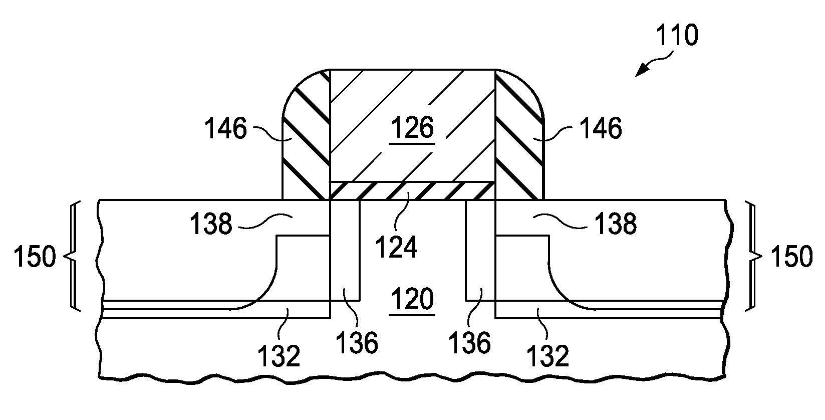
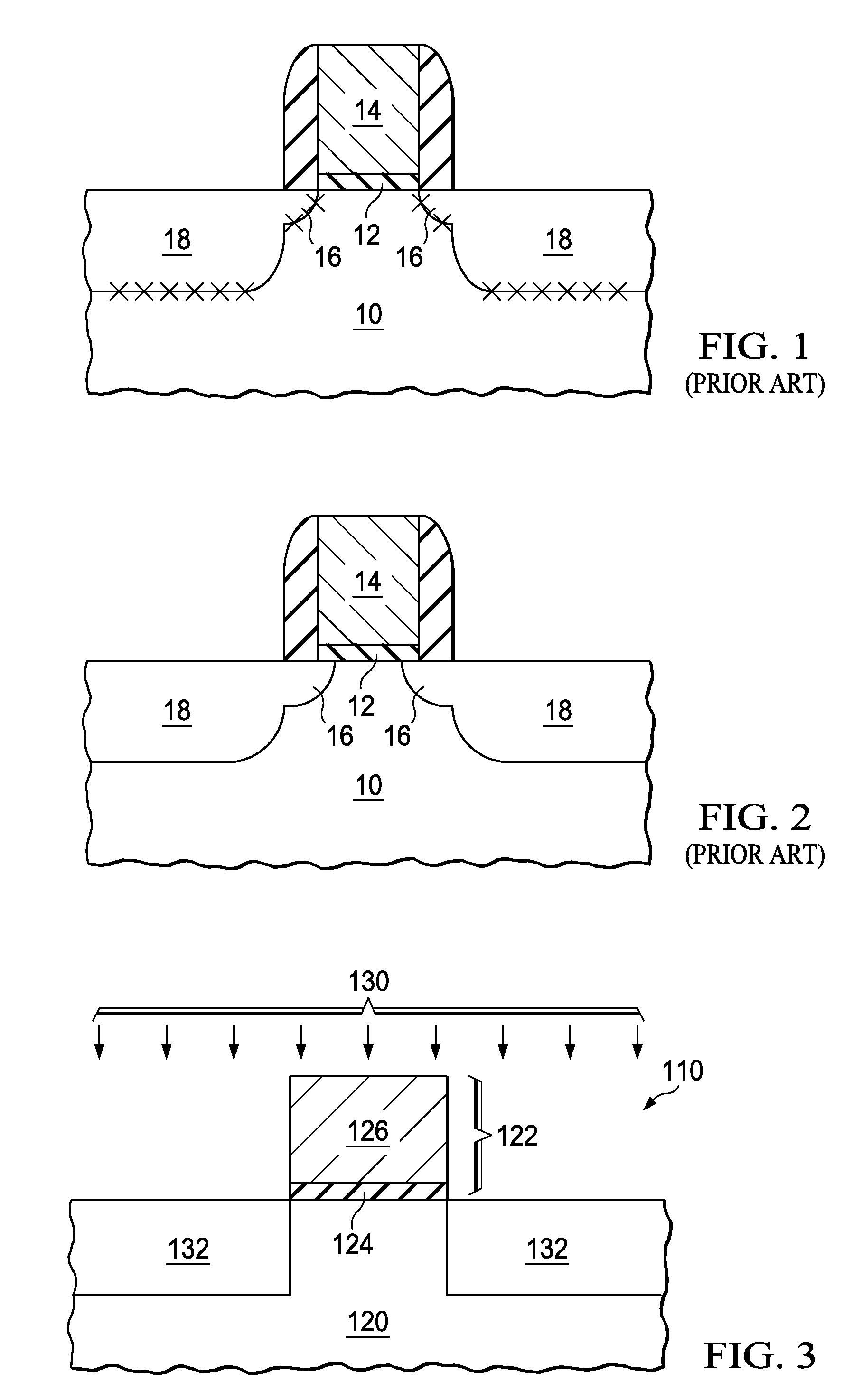
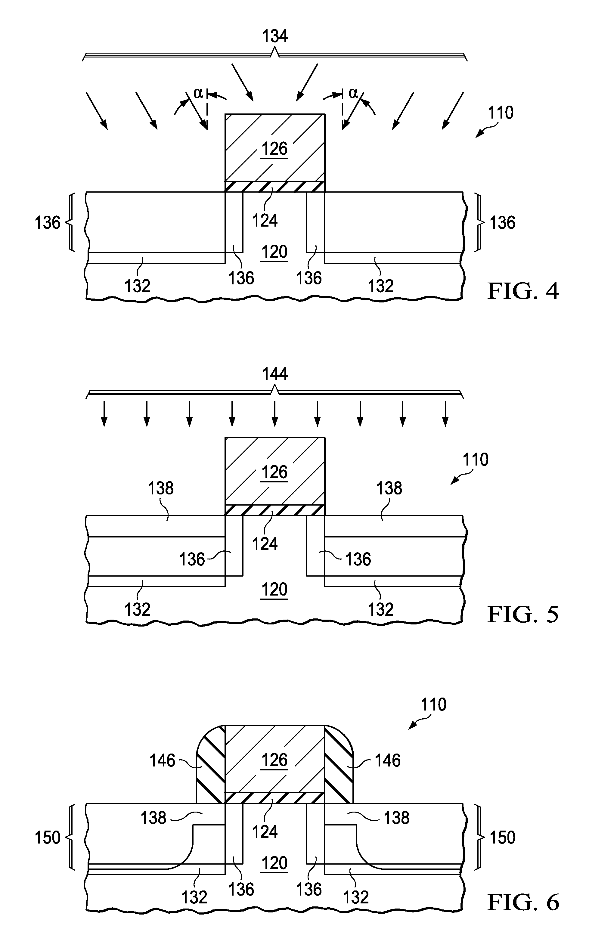
[0017]FIGS. 3 through 6 illustrate the formation of a metal-oxide-semiconductor (MOS) device, which may be a p-type MOS (PMOS) device or an n-typ...


PUM

PropertyMeasurementUnit
temperatureaaaaaaaaaa
temperaturesaaaaaaaaaa
peak temperatureaaaaaaaaaa

Abstract

An annealing method includes performing an activation annealing on a wafer with a peak temperature of greater than about 1200° C., wherein the activation annealing has a first duration; and performing a defect-recovery annealing on the wafer at a defect-recovery temperature lower than the peak temperature for a second duration. The second duration is longer than the first duration. The annealing method includes no additional annealing steps at temperatures greater than about 1200° C., and no room-temperature cooling step exists between the activation annealing and the defect-recovery annealing.

Description

[0001]This application claims the benefit of U.S. Provisional Application No. 61 / 153,914 filed on Feb. 19, 2009, entitled “Junction Profile Engineering Using Staged Thermal Annealing,” which application is hereby incorporated herein by reference.TECHNICAL FIELD[0002]This invention relates generally to semiconductor devices, and more particularly to the thermal annealing of source and drain junctions, and even more particularly to methods for improving activation rates and reducing the diffusion of implanted ions in source and drain regions.BACKGROUND[0003]Metal-oxide-semiconductor (MOS) devices include source and drain regions, which are often formed by implantations. After the implantations, an anneal step(s) needs to be performed. The annealing step has several functions. First, the ions introduced into the source and drain regions need to be activated to reduce the series' resistances in the source and drain regions. Second, the implantation causes the destruction of the lattice ...

Claims


Application Information

Patent Timeline
Patent Type & Authority Applications(United States)
IPC IPC(8): H01L21/336
CPCH01L21/26506H01L21/26513H01L21/26586H01L29/7833H01L29/1083H01L29/6659H01L21/324
Inventor WANG, LI-TINGKU, KEH-CHIANGLIN, YU-CHANGCHENG, NAI-HANHUANG, LI-PING
Owner TAIWAN SEMICON MFG CO LTD
Why Eureka
Try Eureka