
Profile Design for Lateral-Vertical Bipolar Junction Transistor

a bipolar junction transistor and profile design technology, applied in the direction of transistors, semiconductor devices, electrical equipment, etc., can solve the problems of increasing the parasitic effect of lateral-bjts, increasing the cost of lateral-bjts, and reducing so as to reduce the parasitic effect of vertical-bjts and improve current gain

Active Publication Date: 2010-08-26
TAIWAN SEMICON MFG CO LTD
View PDF27 Cites 19 Cited by
  • Summary
  • Abstract
  • Description
  • Claims
  • Application Information

AI Technical Summary

Benefits of technology

[0010]The preferred embodiments of the present invention have improved current gain due to small emitter size, which reduces the parasitic effects of vertical-BJTs.

Problems solved by technology

The ability for improving the gain of conventional vertical-BJTs and lateral-BJTs is limited for the following reasons.
A great length LE and a small area for emitter E are conflicting requirements, which means that the improvement of the lateral-BJT comes with the cost of a greater parasitic BJT.
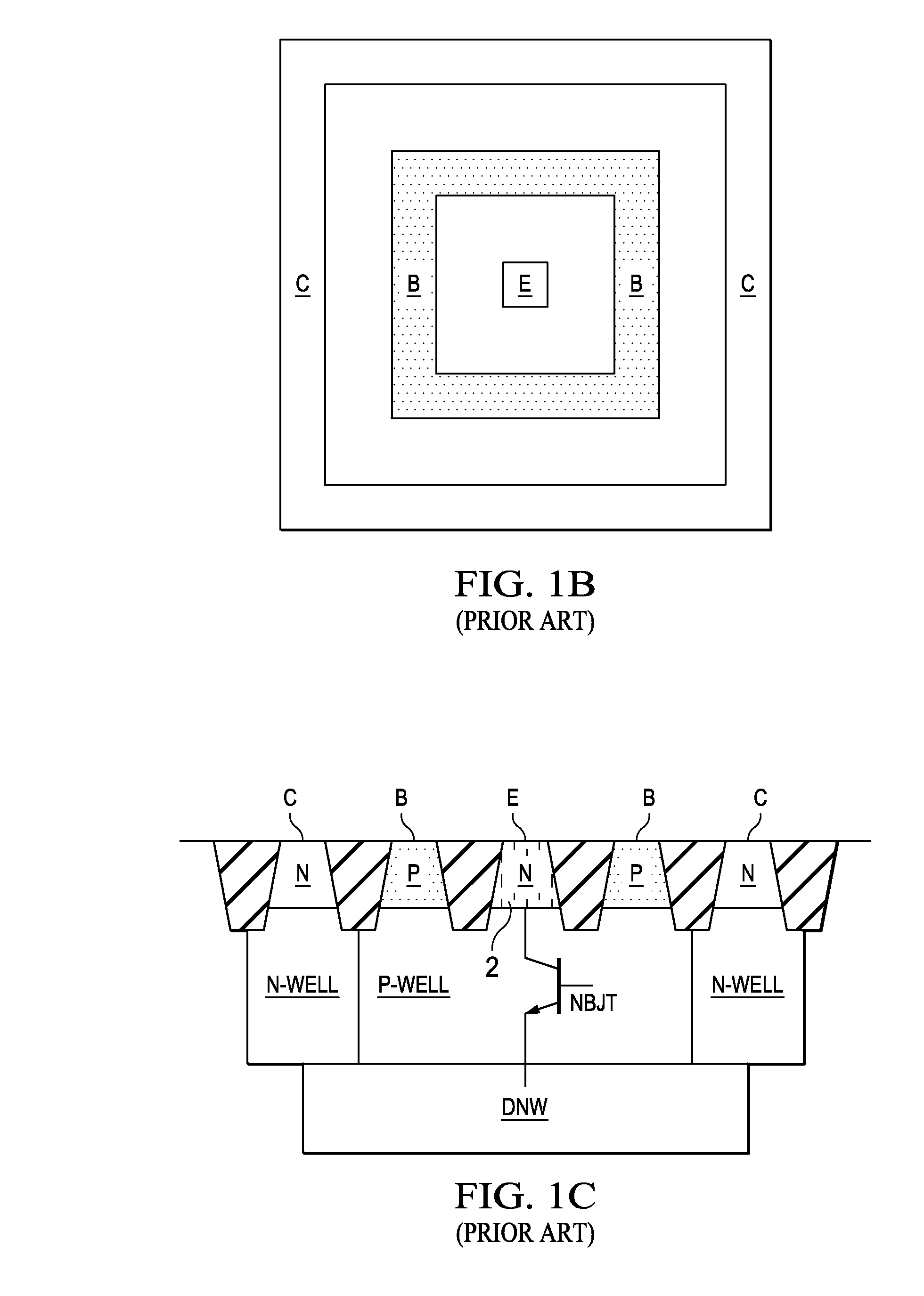
A dilemma for conventional vertical-BJTs is that the base width, which is substantially equal to a depth of the P-well as shown in FIG. 1C, is not scalable, if the vertical-BJTs are formed using a same technology as the formation of CMOS devices.
The pocket implants result in an increase in the dosage in the base regions, hence a decrease in current gain.
Furthermore, the lightly-doped source / drain (LDD) implants cause a gradient dose profile at base / emitter junctions, resulting in lower emitter injection efficiency.

Method used


Image

  • Profile Design for Lateral-Vertical Bipolar Junction Transistor
  • Profile Design for Lateral-Vertical Bipolar Junction Transistor
  • Profile Design for Lateral-Vertical Bipolar Junction Transistor

Examples


Embodiment Construction

[0022]The making and using of the presently preferred embodiments are discussed in detail below. It should be appreciated, however, that the present invention provides many applicable inventive concepts that can be embodied in a wide variety of specific contexts. The specific embodiments discussed are merely illustrative of specific ways to make and use the invention, and do not limit the scope of the invention.

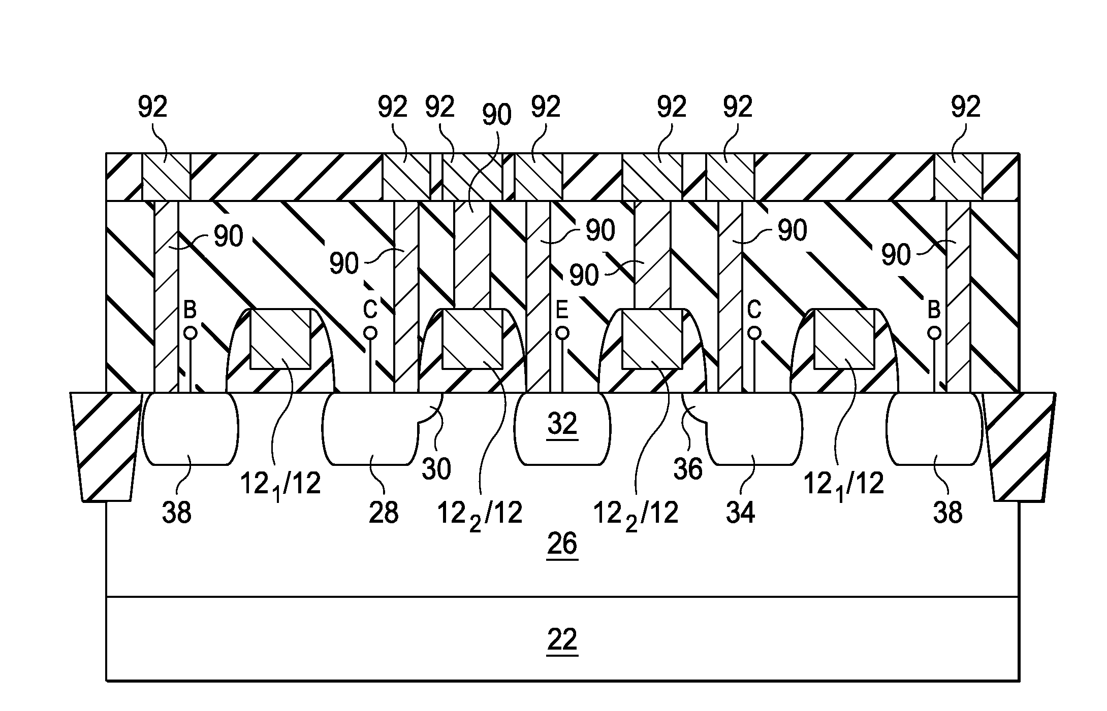
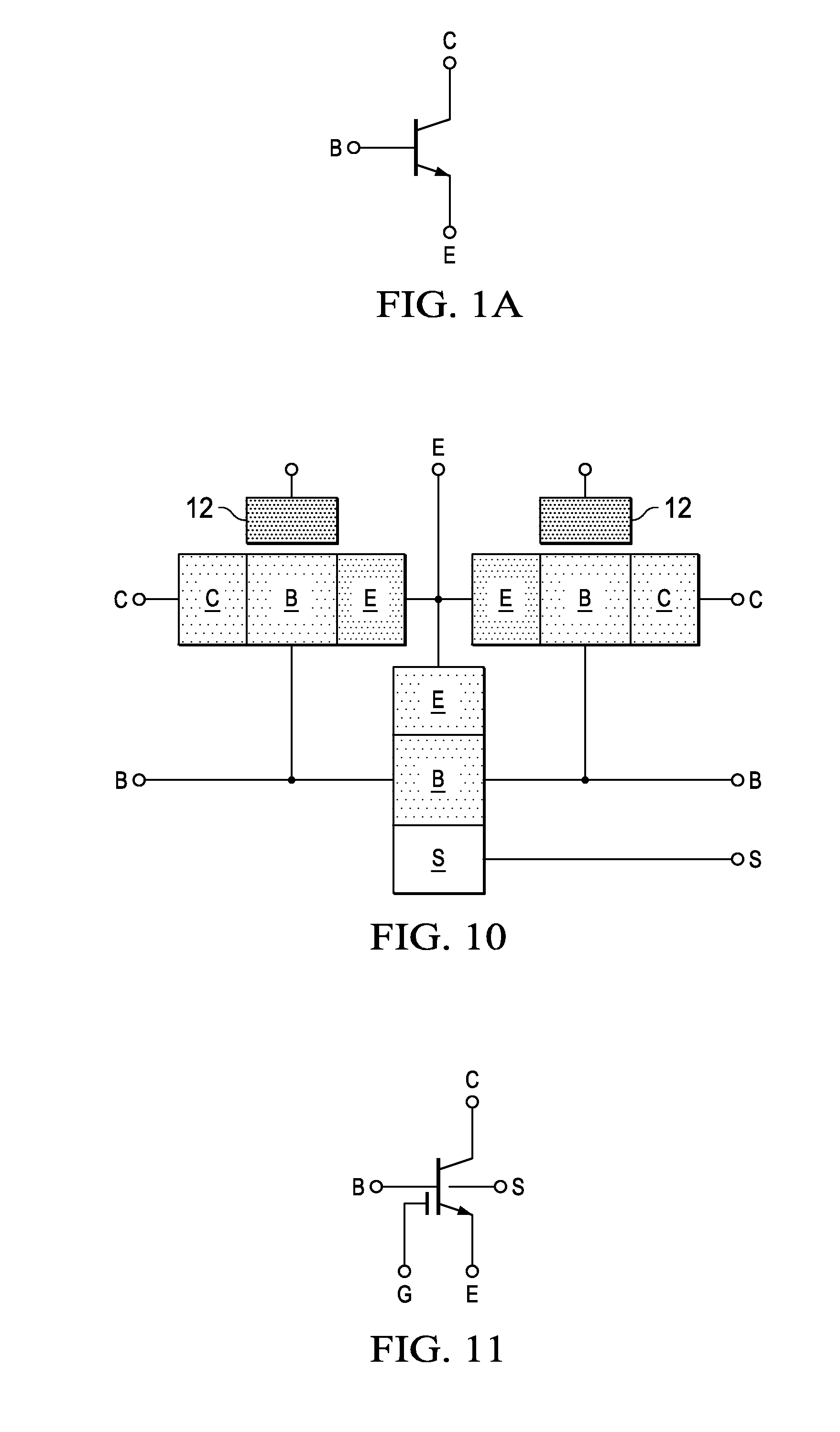
[0023]A novel design of lateral-vertical bipolar junction transistors (LVBJTs) having improved current gain is provided. The preferred embodiments are illustrated. The variations of the preferred embodiments are then discussed. Throughout the various views and illustrative embodiments of the present invention, like reference numbers are used to designate like elements.

[0024]In order to design a high current-gain LVBJT, several principles are preferably applied. The base width, which is the distance in the base region separating an emitter and a collector, is preferably minimi...


PUM


Abstract

A lateral-vertical bipolar junction transistor (LVBJT) includes a well region of a first conductivity type over a substrate; a first dielectric over the well region; and a first electrode over the first dielectric. A collector of a second conductivity type opposite the first conductivity type is in the well region and on a first side of the first electrode, and is adjacent the first electrode. An emitter of the second conductivity type is in the well region and on a second side of the first electrode, and is adjacent the first electrode, wherein the second side is opposite the first side. A collector extension region having a lower impurity concentration than the collector adjoins the collector and faces the emitter. The LVBJT does not have any emitter extension region facing the collector and adjoining the emitter.

Description

[0001]This application claims priority to provisionally filed U.S. patent application Ser. No. 61 / 187,796, filed Jun. 17, 2009, and entitled “Profile Design for Lateral-Vertical Bipolar Junction Transistor,” and is a continuation-in-part of U.S. patent application Ser. No. 11 / 589,478, filed Oct. 30, 2006, and entitled “High-Gain Vertex Lateral Bipolar Junction Transistor,” which application claims priority to provisionally filed U.S. Patent Application Ser. No. 60 / 731,720, filed Oct. 31, 2005, and entitled “A Novel High-Gain Vertex Lateral-BJT,” which applications are hereby incorporated herein by reference.TECHNICAL FIELD[0002]This invention relates generally to semiconductor devices, and more particularly to the structures and fabrication methods of lateral-vertical bipolar junction transistors.BACKGROUND[0003]Bipolar junction transistors (BJTs) are key parts of analog integrated circuits. BJTs can be grouped as NPN BJTs (NBJTs) and PNP BJTs (PBJTs). A symbol for an NPN BJT, which...

Claims


Application Information

Patent Timeline
Patent Type & Authority Applications(United States)
IPC IPC(8): H01L27/082
CPCH01L21/8224H01L27/0203H01L29/735H01L29/0692H01L27/0821
Inventor CHEN, SHUO-MAOCHAO, CHIH-PINGCHANG, CHIH-SHENGTSENG, HUA-CHOU
Owner TAIWAN SEMICON MFG CO LTD
Learn More