Chip component mounted wiring board

a chip component and wiring board technology, applied in the field of wiring boards, can solve the problems of easy generation of crosstalk noise between the wirings or easy fluctuation of the potential of the power source line or the like, and increase in frequency

Active Publication Date: 2010-08-26
SHINKO ELECTRIC IND CO LTD
View PDF4 Cites 12 Cited by
  • Summary
  • Abstract
  • Description
  • Claims
  • Application Information

AI Technical Summary

Benefits of technology

[0020]Thereby, the wettability of the plated surface of the portion on the terminal electrode is sufficiently secured, so that when the chip component ...

Problems solved by technology

As a result, a problem such as a crosstalk noise generated between the wirings or a fluctuation in the potential of a power source line or the like may occur.
In particular, in a package on which an electronic component such as a semiconductor element requiring a high speed switching operation (such as an MPU) is mounted, an increase in frequency makes a crosstalk noise easy to be generated.
In addition, a high speed on/off operation of a switching element generates a switching noise, which causes the potential of the power source line or the like to easily fluctuate.
In that case, a problem below occurs due to the fact that the Sn plated layers are provided on the surfaces of the termin...

Method used


Image

  • Chip component mounted wiring board
  • Chip component mounted wiring board
  • Chip component mounted wiring board

Examples


first embodiment

; See FIGS. 1 to 5C

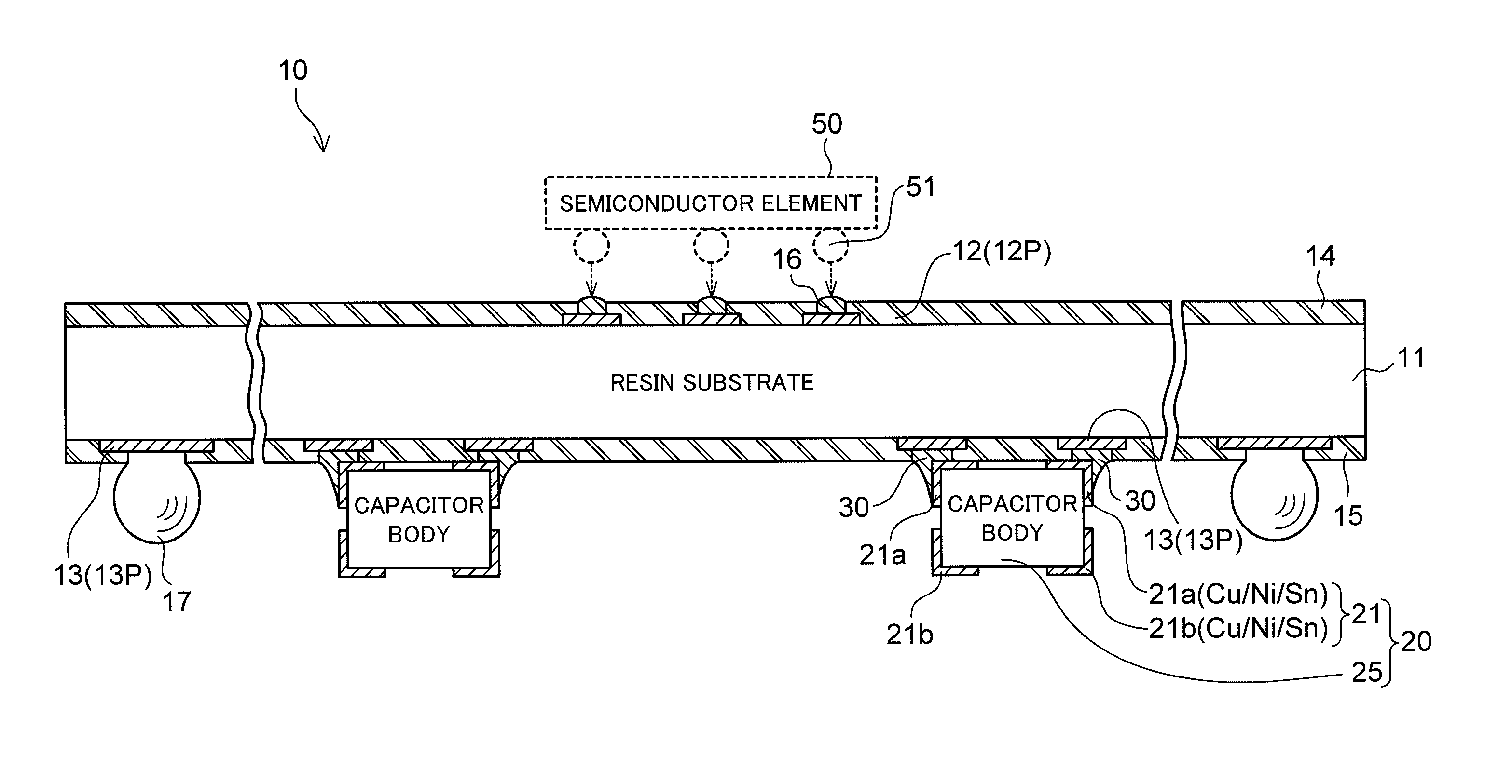
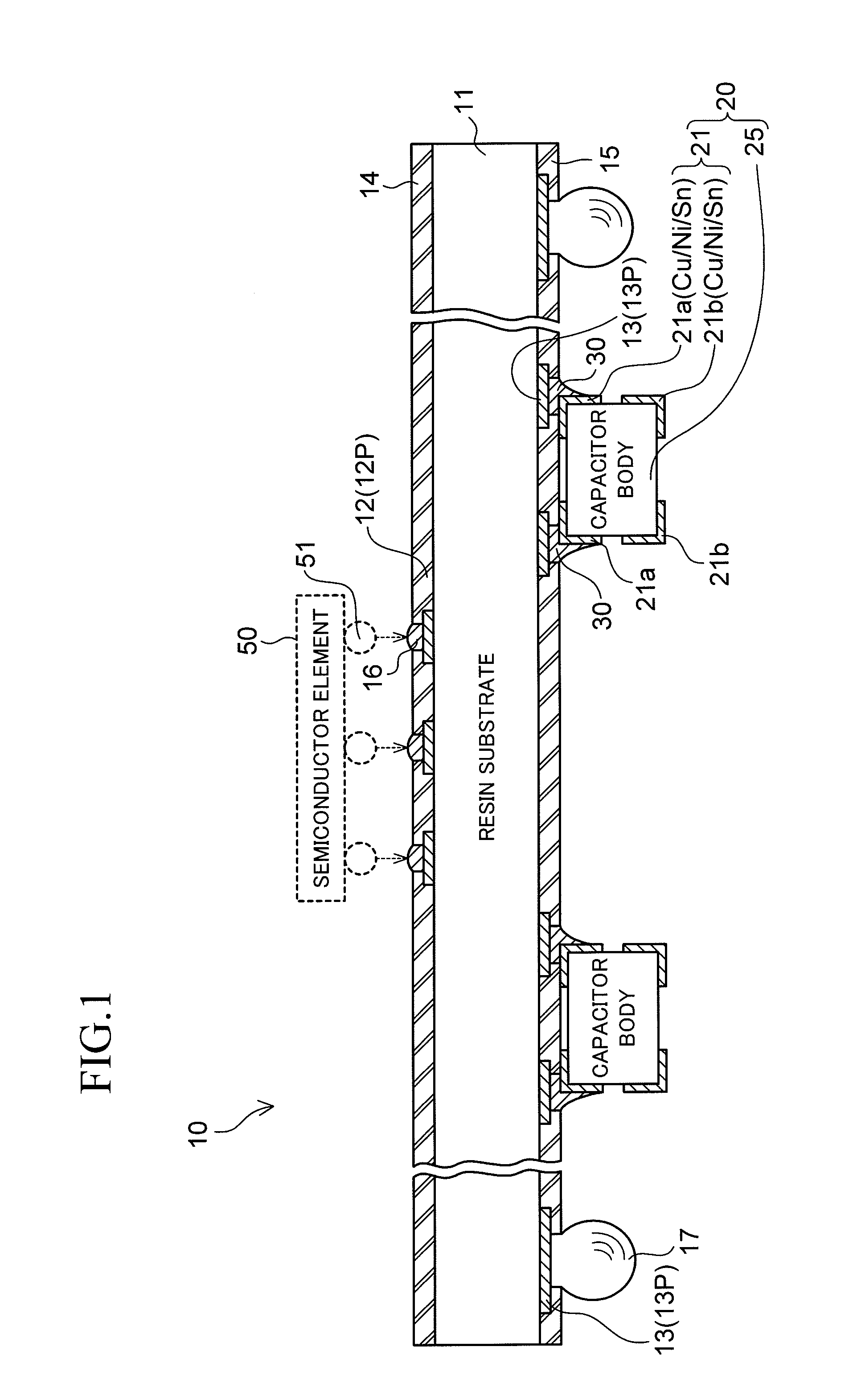
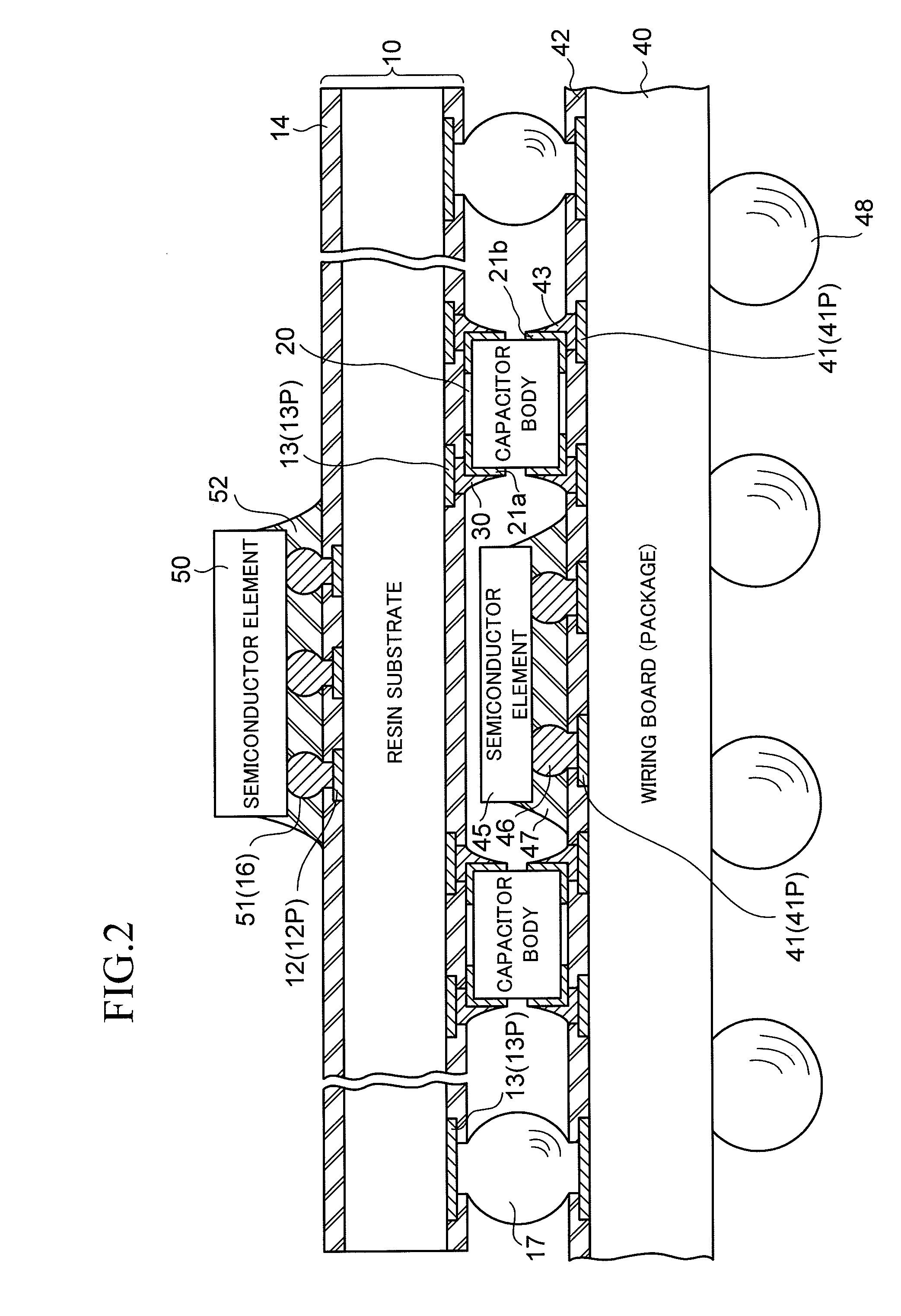
[0032]FIG. 1 shows a configuration of a chip component mounted wiring board (package) 10 according to a first embodiment of the present invention in cross-sectional view. FIG. 2 shows the state where the wiring board (package) 10 is mounted on the other wiring board (package 40) (mounting structure of POP bonding) in cross-sectional view. Moreover, FIGS. 3A and 3B show a configuration of a chip component (chip capacitor 20) surface-mounted on the package (wiring board 10). FIG. 3A shows the appearance (perspective view) of the chip capacitor 20, and FIG. 3B shows a vertical cross-sectional structure when viewed along the line A-A of FIG. 3A.

[0033]As shown in FIG. 1, in the chip component mounted wiring board (package) 10 of the present embodiment, reference numeral 11 denotes a resin substrate forming the body of the wiring board, and reference numerals 12 and 13 denote wiring layers patterned and formed in required shapes on both surfaces of the resin substrate 1...

second embodiment

; See FIGS. 6 to 9

[0072]FIG. 6 shows a configuration of a chip component mounted wiring board (package) 10a according to a second embodiment of the present invention in cross-sectional view. FIG. 7 shows the state where the wiring board (package) 10a is mounted on the other wiring board (package 40) (mounting structure of POP bonding) in cross-sectional view. Moreover, FIGS. 8A and 8B show a configuration of a chip component (chip capacitor 20a) surface-mounted on the package (wiring board 10a). FIG. 8A shows the appearance (perspective view) of the chip capacitor 20a, and FIG. 8B shows a vertical cross-sectional structure when viewed along the line A-A of FIG. 8A.

[0073]The configuration of the chip component mounted wiring board (package) 10a according to the second embodiment (FIGS. 6 to 9) is different from that of the chip component mounted wiring board (package) 10 according to the first embodiment (FIGS. 1 to 3B) in the following points. Instead of vertically separating the te...


PUM


Abstract

A wiring board to be used with being mounted on a packaging board includes a chip component surface-mounted on a surface facing the packaging board. The chip component includes terminal electrodes at both end portions of the component body thereof. Each of the terminal electrodes is provided in a form in which a plated film (Sn) formed on the surface of the terminal electrode is separated into two portions, one portion being on the wiring board side, and another portion being on the packaging board side. In one aspect, each of the terminal electrodes of the chip component is separated into a portion on the wiring board side and a portion on the packaging board side, and the plated film (Sn) is formed on a surface of each of the separated portions of each of the terminal electrodes.

Description

CROSS-REFERENCE TO RELATED APPLICATIONS[0001]This application is based on and claims priority of Japanese Patent Application No. 2009-040176 filed on Feb. 24, 2009, the entire contents of which are incorporated herein by reference.BACKGROUND OF THE INVENTION[0002](a) Field of the Invention[0003]The present invention relates to a wiring board to be used with being mounted on a packaging board such as an interposer or another wiring board. More specifically, the invention relates to a chip component mounted wiring board including a passive device (chip component) such as a chip-shaped capacitor or inductor surface-mounted on the surface facing the packaging board.[0004]The aforementioned chip component mounted wiring board is also referred to as a “semiconductor package” or simply as a “package” in the description below for the sake of convenience, because it has the role as a package for mounting an electronic component such as a semiconductor element on the surface opposite to the s...

Claims


Application Information

Patent Timeline
IPC IPC(8): H05K1/18
CPCH05K1/0231H05K1/144H01L2924/01322H01L2924/19106H01L2924/19105H01L2924/15331H01L2924/15311H01L2224/73204H01L2224/32225H01L2224/16225H01L25/105H05K2201/10636H05K1/145H05K3/3442H01L2924/00012H01L2924/00Y02P70/50
Inventor AOKI, TOSHIAKIEBE, MASAYOSHISHIMADA, KIYOTAKA
Owner SHINKO ELECTRIC IND CO LTD
Why Eureka
Try Eureka