Pixel sensor cell including light shield

a technology of light shield and sensor cell, applied in the field of pixel sensor cell, to achieve the effect of avoiding spurious light effects

Active Publication Date: 2010-09-16
GLOBALFOUNDRIES US INC
View PDF13 Cites 69 Cited by
  • Summary
  • Abstract
  • Description
  • Claims
  • Application Information

AI Technical Summary

Benefits of technology

[0015]This invention teaches a structure to create a light shield which will work for a back side illuminated imager thus allowing for the creation of a global shutter back side illuminated imager. More particularly, the invention provides a pixel sensor cell, a method for fabricating the pixel sensor cell and a design structure for fabricating the pixel sensor cell. The pixel sensor cell, which includes therein a light blocking layer, typically but not exclusively, comprises a complementary metal oxide semiconductor (CMOS) pixel sensor cell. Within a particular embodiment, the light blocking layer is located interposed between a first semiconductor layer spaced further from a carrier

Problems solved by technology

The back side illuminated imager technology is not often combined with the global shutter imager technology due to the difficult

Method used


Image

  • Pixel sensor cell including light shield
  • Pixel sensor cell including light shield
  • Pixel sensor cell including light shield

Examples


Embodiment Construction

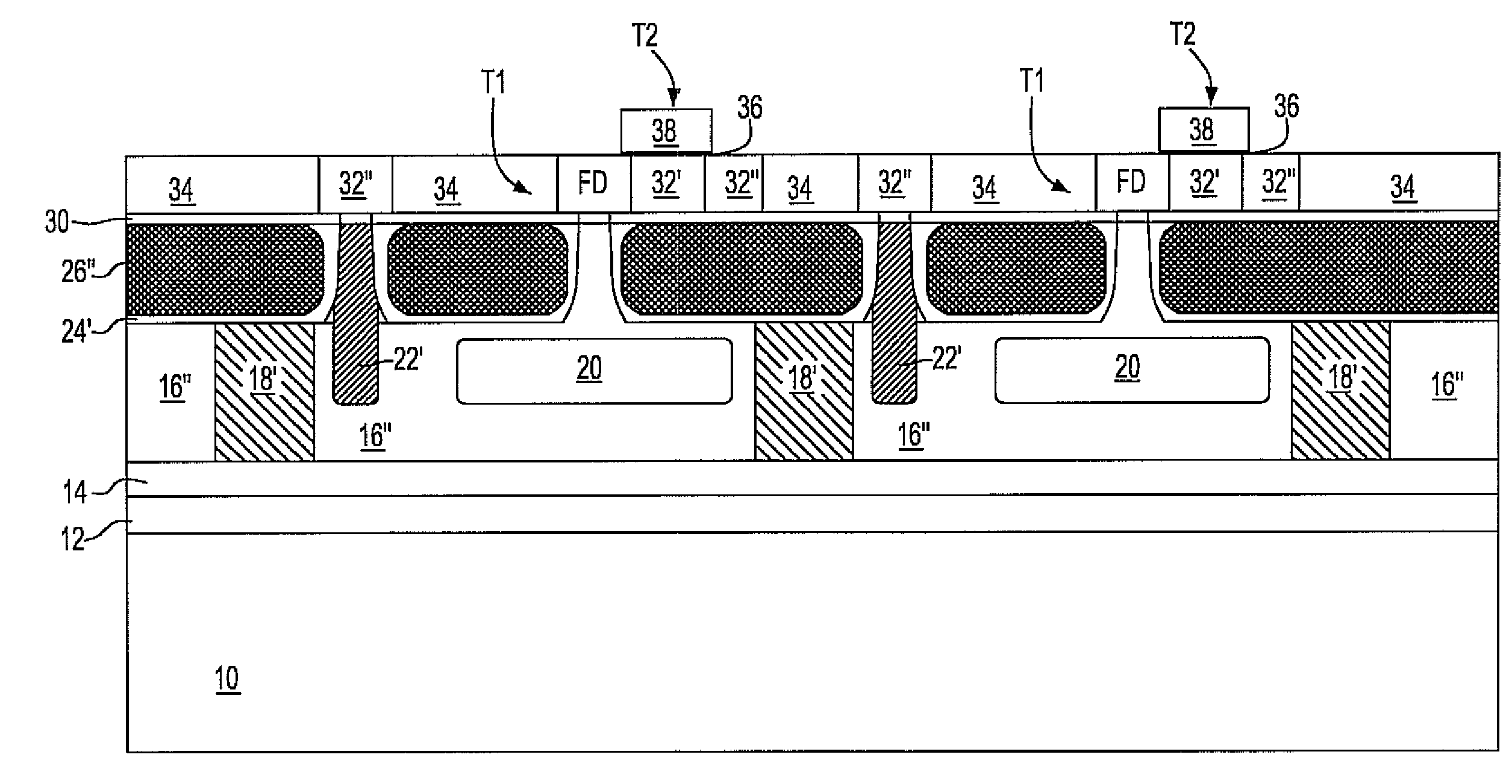
[0031]The invention, which includes a pixel sensor cell, a method for fabricating the pixel sensor cell and a design structure for fabricating the pixel sensor cell, is understood within the context of the description set forth below. The description set forth below is understood within the context of the drawings described above. Since the drawings are intended for illustrative purposes, the drawings are not necessarily drawn to scale.

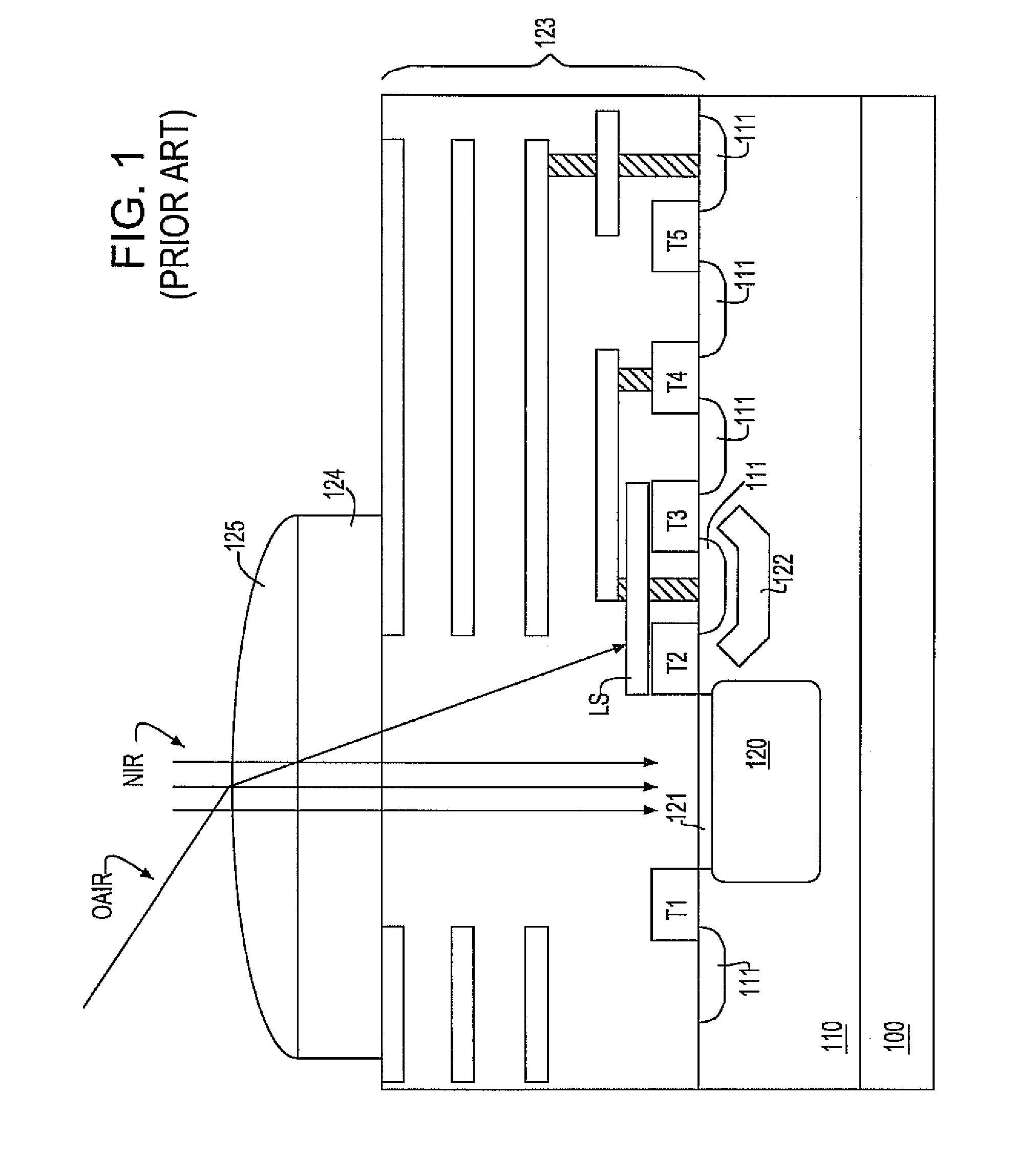
[0032]FIG. 1 shows the prior art for a CMOS global shutter imaging pixel. FIG. 1 shows a semiconductor substrate 100 and an epitaxial layer 110 located upon the semiconductor substrate 100. Included within the epitaxial layer 110 are transistor structures T1, T2, T3, T4 and T5 that include source / drain regions 111. Source / drain region 111 interposed between transistor T2 and transistor T3 serves as a floating diffusion with a charge collection shield 122 therebeneath. Also located upon the epitaxial layer 110 and covering the transistor structures T1 ...


PUM


Abstract

CMOS image sensor pixel sensor cells, methods for fabricating the pixel sensor cells and design structures for fabricating the pixel sensor cells are designed to allow for back side illumination in global shutter mode by providing light shielding from back side illumination of at least one transistor within the pixel sensor cells. In a first particular generalized embodiment, a light shielding layer is located and formed interposed between a first semiconductor layer that includes a photoactive region and a second semiconductor layer that includes the at least a second transistor, or a floating diffusion, that is shielded by the light blocking layer. In a second generalized embodiment, a thin film transistor and a metal-insulator-metal capacitor are used in place of a floating diffusion, and located shielded in a dielectric isolated metallization stack over a carrier substrate

Description

[0001]Applicant claims the benefit of Provisional Application Ser. No. 61 / 158,769, Pixel Sensor Cell Including Light Shield, filed on Mar. 10, 2009.BACKGROUND[0002]The invention relates generally to pixel sensor cells, methods for fabrication thereof and design structures for fabrication thereof. More particularly, the invention relates to back side illuminated pixel sensor cells intended for use in global shutter mode, with enhanced light shielding.[0003]Solid state sensors are popular optoelectronic components that find use in various technology applications, including in particular imaging technology applications. Particularly common are solid state sensors that are used as active light capture and imaging elements within digital cameras.[0004]Solid state image sensors may be fabricated using any of several semiconductor technologies for the active light capture and imaging elements. Charge coupled devices are known as more traditional solid state image sensor light capture and i...

Claims


Application Information

Patent Timeline
IPC IPC(8): H01L27/148H01L27/146H01L31/0216H01L21/30G06F17/50
CPCH01L27/14609H01L27/1464H01L27/14689H01L27/14623
Inventor ELLIS-MONAGHAN, JOHNGAMBINO, JEFFREY P.JAFFE, MARK D.RASSEL, RICHARD J.
Owner GLOBALFOUNDRIES US INC
Why Eureka
Try Eureka