
Reflective electrode, display device, and method for producing display device

a technology of display device and reflector, which is applied in the manufacture of electrode systems, instruments, non-electron-emitting electrode materials, etc., can solve the problems of low reflectance of high-melting-point metals such as mo and cr, increase production cost and productivity, and reduce contact resistance, etc., to achieve high reflectance, low contact resistance, and high reflectance

Inactive Publication Date: 2010-09-16
KOBE STEEL LTD
View PDF41 Cites 29 Cited by
  • Summary
  • Abstract
  • Description
  • Claims
  • Application Information

AI Technical Summary

Benefits of technology

[0040]The reflective electrodes according to the present invention each have an aluminum oxide layer containing O (oxygen) in a less amount and being thin in a contact area with the transparent pixel electrode. They therefore excel in all properties such as reflection properties, contact resistance, electric resistivity, and thermal stability even when the aluminum oxide layer constituting the reflective electrodes is directly connected to the electroconductive oxide film constituting the transparent electrode without the interposition of a barrier metal layer, in contrast to common techniques. Specifically, for example, the reflective electrodes have high reflectances and low contact resistances and do not cause defects such as hillocks even after subjected to a heat treatment at a low temperature of about 100° C. or higher and 300° C. or lower. Accordingly, the reflective electrodes according to the present invention, when used, can provide display devices having excellent productivity, being inexpensive, and showing high performance.

Problems solved by technology

However, the high-melting-point metals such as Mo and Cr have very low reflectances.
In addition, strong demands have been made to develop wiring materials for reflective electrodes, which can reduce the contact resistance even when omitting the barrier metal layer.
This is because the deposition of the barrier metal layer needs extra installation of a deposition chamber for the deposition of the barrier metal, in addition to a deposition sputtering system required for the deposition of the transparent pixel electrode; but such increase in production cost and decrease in productivity accompanied with the formation of the barrier metal layer become not neglectable as the cost reduction proceeds with commercial production of such liquid crystal panels.
The use of barrier metal layer further increases the cost.

Method used


Image

  • Reflective electrode, display device, and method for producing display device
  • Reflective electrode, display device, and method for producing display device
  • Reflective electrode, display device, and method for producing display device

Examples


experimental example 1

[0133]The first production method was investigated in this experimental example.

[0134]Specifically, a series of layer of Al—Ni—La alloys as materials for a reflective electrode was deposited through sputter deposition each on an alkali-free glass plate (thickness (gauge) 0.7 mm) substrate. The sputter deposition was performed under conditions of an Ar atmosphere at a pressure of 1 mTorr and a power of 100 W. In each sample, the thickness of the Al—Ni—La alloy layer was controlled to be about 100 nm. The Ni contents and La contents in the Al—Ni—La alloy layers are shown in Table 1.

[0135]Next, samples of the Al—Ni—La alloy layers were divided into two groups, i.e., those subjected to a heat treatment and those not subjected to a heat treatment. The heat treatment was performed at a temperature given in Table 1 in a vacuum atmosphere (with a degree of vacuum of equal to or less than 3×10⁻⁴ Pa) or in a N2 atmosphere for 1 hour.

[0136]Next, non-treated and heat-treated Al—Ni—La alloy laye...

experimental example 2

[0145]The second production method was investigated in this experimental example.

[0146]Specifically, samples according to the present invention (Examples) were prepared by depositing an Al—Ni—La alloy layer (thickness: about 100 nm) and an ITO film (thickness: about 50 nm) on an alkali-free glass plate (thickness (gauge) 0.7 mm) by the procedure of Experimental Example 1, except for not performing a heat treatment but performing the deposition of ITO while using an Ar sputtering gas further containing 12% of N2 gas in terms of ratio by volume flow rate. For comparison, comparative samples (Comparative Examples) were prepared by performing the deposition of ITO in an atmosphere of Ar gas alone.

[0147]Of these samples according to the present invention and comparative samples, the contact resistance, and the [O] / [Al] ratios and thickness in its thinnest portion of the aluminum oxide layer were measured by the procedure of Experimental Example 1.

[0148]As a result, the samples according ...

experimental example 3

[0149]The third production method was investigated in this experimental example.

[0150]Specifically, an Al—Ni—La alloy layer (thickness: about 100 nm) and an ITO film (thickness: about 50 nm) were deposited on an alkali-free glass plate (thickness (gauge) 0.7 mm) by the procedure of Experimental Example 1, except for not performing the heat treatment. Instead of the heat treatment, samples were placed in a sputter deposition system for ITO film, Ar gas was introduced in the system, and the sample surfaces were subjected to reverse sputtering with Ar for 10 seconds while changing (reversing) the polarity of sputtering. The reverse sputtering was performed under conditions of Ar atmosphere at a pressure of 1 mmTorr and a power of 100 W. Thereafter the polarity of sputtering was turned back, and an ITO film was deposited by the procedure of Experimental Example 1 and thereby yielded samples according to the present invention. For comparison, comparative samples were prepared without per...


PUM


Abstract

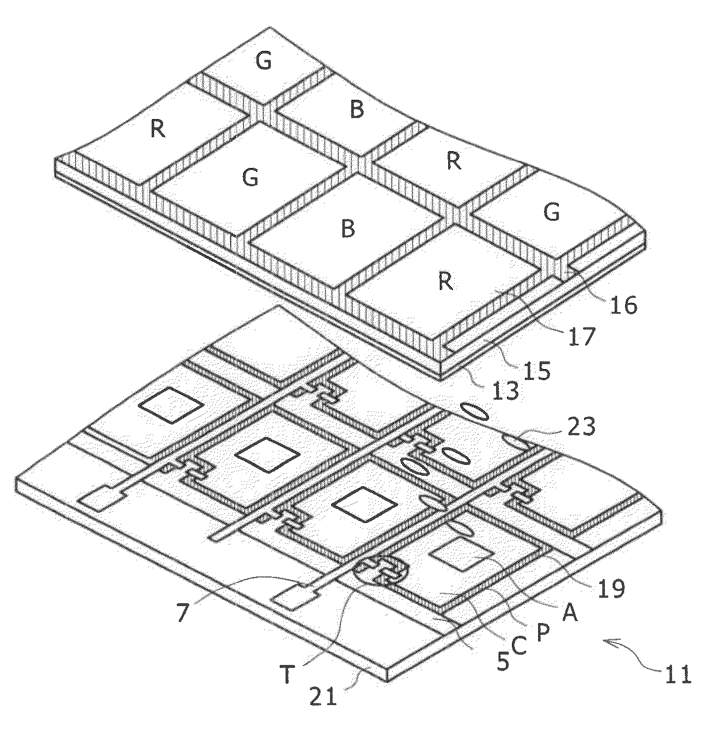
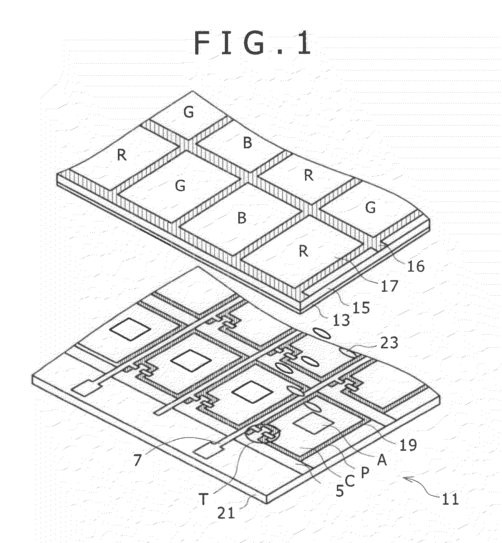
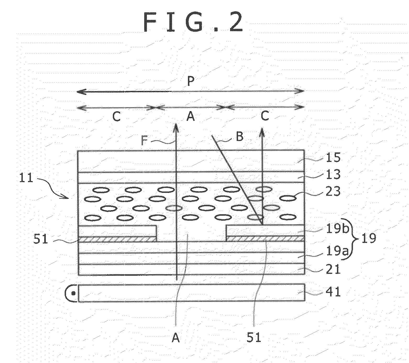
A reflective electrode (2) includes an aluminum alloy layer (2a) and an aluminum oxide layer (2b) arranged on or above a substrate and is directly connected to a transparent pixel electrode (3) without the interposition of a barrier metal layer. The aluminum alloy layer contains 0.1 to 2 atomic percent of nickel or cobalt and 0.1 to 2 atomic percent of lanthanum. The aluminum oxide layer has a ratio [O] / [Al] of the number of oxygen atoms [O] to the number of aluminum atoms [Al] of 0.30 or less. The aluminum oxide layer has a thickness in its thinnest portion of 10 nm or less. The reflective electrode has a high reflectance and a low contact resistance, even when subjected to a heat treatment at a low temperature of 100° C. or higher but 300° C. or lower. The reflective electrode also has excellent thermal stability and does not cause defects such as hillocks.

Description

TECHNICAL FIELD[0001]The present invention relates to reflective electrode for use in display devices represented by liquid crystal displays and organic electroluminescent (EL) displays; to display devices including the reflective electrodes; and production methods of the display devices. Hereinafter the present invention will be illustrated by taking liquid crystal displays as representative examples; but it should be noted that these are never construed to limit the scope of the present invention.BACKGROUND ART[0002]Liquid crystal displays are broadly grouped under transmissive display devices, reflective display devices, and semi-transmissive display devices. The transmissive display devices adopt, as a light source, light from a lighting unit (back light) arranged at the rear of a liquid crystal panel. The reflective display devices adopt, as a light source, surrounding light. The semi-transmissive display devices have properties both as transmissive ones and reflective ones.[00...

Claims


Application Information

Patent Timeline
IPC IPC(8): H01J1/02H01J9/02
CPCG02B5/0833G02F1/133553H01L51/5203H01L27/3244G02F1/133555H10K59/805H10K50/805H10K59/12
Inventor OCHI, MOTOTAKAGOTO, HIROSHI
Owner KOBE STEEL LTD
Learn More