Controlled localized defect paths for resistive memories

a localized defect and resistive memory technology, applied in the field of semiconductor devices, can solve the problems of limited utility and slowness of memories

Active Publication Date: 2010-09-30
INTERMOLECULAR
View PDF48 Cites 192 Cited by
  • Summary
  • Abstract
  • Description
  • Claims
  • Application Information

AI Technical Summary

Problems solved by technology

These memories can be slow and are therefore of limited utility as t...

Method used


Image

  • Controlled localized defect paths for resistive memories
  • Controlled localized defect paths for resistive memories
  • Controlled localized defect paths for resistive memories

Examples


Embodiment Construction

[0019]A detailed description of one or more embodiments is provided below along with accompanying figures. The detailed description is provided in connection with such embodiments, but is not limited to any particular example. The scope is limited only by the claims and numerous alternatives, modifications, and equivalents are encompassed. Numerous specific details are set forth in the following description in order to provide a thorough understanding. These details are provided for the purpose of example and the described techniques may be practiced according to the claims without some or all of these specific details. For the purpose of clarity, technical material that is known in the technical fields related to the embodiments has not been described in detail to avoid unnecessarily obscuring the description.

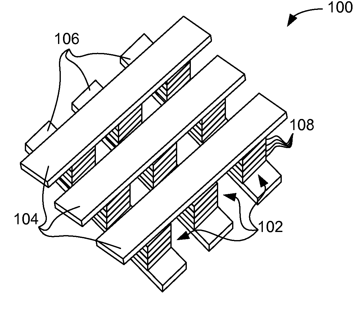
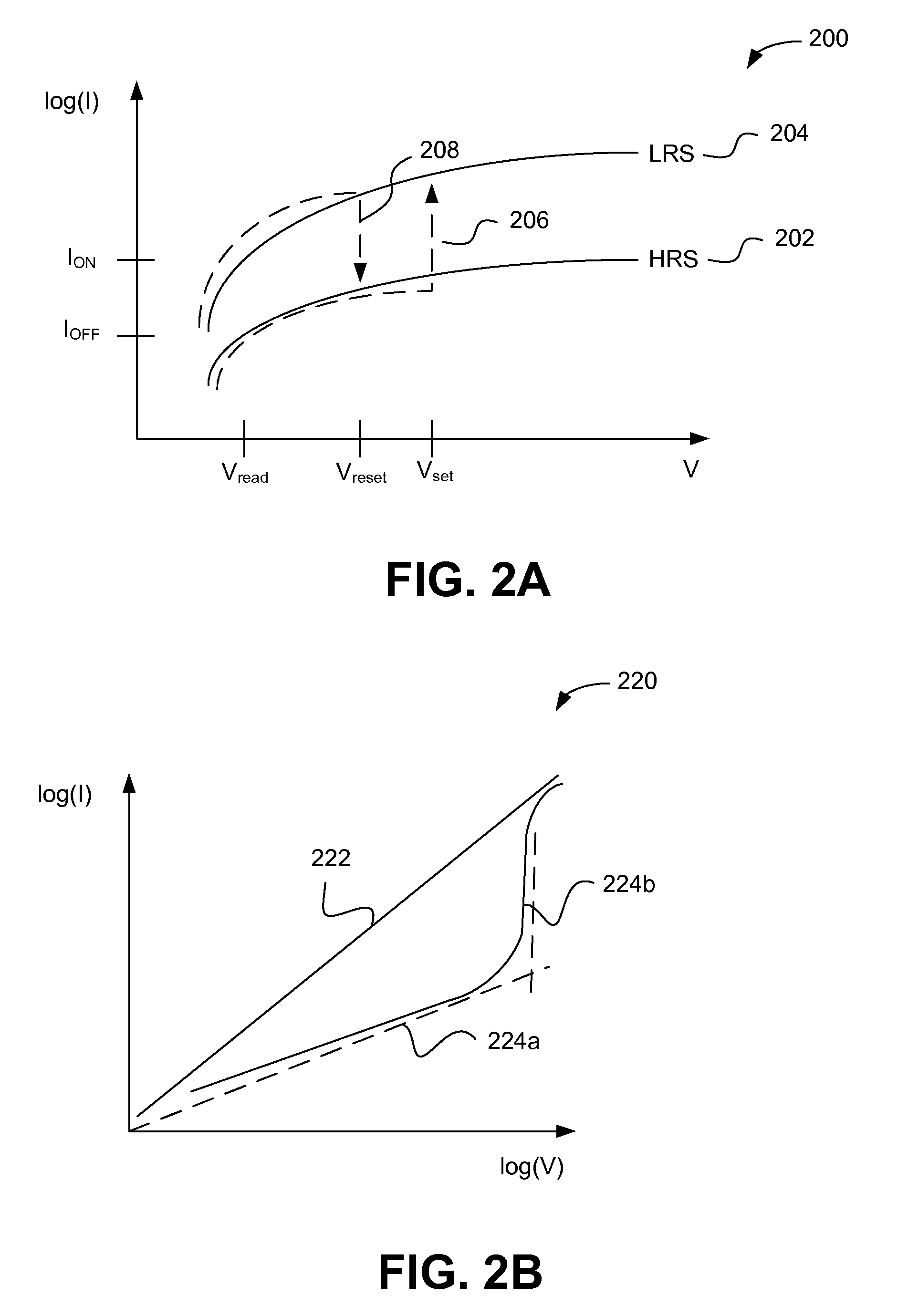
[0020]According to various embodiments, a resistive switching nonvolatile memory including controlled localized defect paths is described. Switching parameters of the memory c...


PUM


Abstract

Controlled localized defect paths for resistive memories are described, including a method for forming controlled localized defect paths including forming a first electrode forming a metal oxide layer on the first electrode, masking the metal oxide to create exposed regions and concealed regions of a surface of the metal oxide, and altering the exposed regions of the metal oxide to create localized defect paths beneath the exposed regions.

Description

PRIORITY CLAIM TO PROVISIONAL APPLICATION[0001]A claim for priority is hereby made under the provisions of 35 U.S.C. §119 for the present application based upon U.S. Provisional Application No. 61 / 165,407 entitled “Controlled Localized Defect Paths for Resistive Memories” and filed on Mar. 31, 2009, which is incorporated herein by reference.FIELD OF THE INVENTION[0002]The present invention relates generally to semiconductor memories. More specifically, controlled localized defect paths for resistive memories are described.BACKGROUND OF THE INVENTION[0003]Nonvolatile memories are memories that retain their contents even when unpowered. Nonvolatile memories have a variety of uses, from storage for portable devices to rewriteable memories in embedded systems. Several types of nonvolatile memories are commonly available, including electronically erasable programmable read only memory (EEPROM)-type memories such as flash memory. These memories can be slow and are therefore of limited uti...

Claims


Application Information

Patent Timeline
IPC IPC(8): H01L47/00H01L21/16
CPCG11C13/0007H01L45/122G11C2213/55G11C2213/56H01L21/265H01L21/322H01L27/2463H01L45/08H01L45/10H01L45/1233H01L45/146H01L45/1616H01L45/1625H01L45/1641H01L45/165H01L45/1658H01L45/1675H01L45/12H01L45/1246G11C2213/32H10B63/80H10N70/25H10N70/24H10N70/828H10N70/023H10N70/041H10N70/043H10N70/026H10N70/046H10N70/826H10N70/8833H10N70/063H10N70/8836H10N70/821H10N70/801
Inventor CHIANG, TONYMILLER, MICHAELPHATAK, PRASHANT
Owner INTERMOLECULAR
Why Eureka
Try Eureka