Semiconductor device

a technology of semiconductors and devices, applied in semiconductor devices, electrical devices, transistors, etc., can solve problems such as disadvantageous cracks, and achieve the effects of suppressing cracks, reducing the change amount of lattice constants, and improving the stress relaxation effect of the second composition graded layer

Active Publication Date: 2010-09-30
SANKEN ELECTRIC CO LTD
View PDF1 Cites 68 Cited by
  • Summary
  • Abstract
  • Description
  • Claims
  • Application Information

AI Technical Summary

Benefits of technology

[0016]According to the present invention, the second composition graded layer composition-graded to the first nitride-based semiconductor layer that causes a tensile stress is made thick, thereby reducing a change amount of a lattice constant of the second composition graded layer. As a result, a stress relaxing effect of the second composition graded layer can be improved and damage such as cracks can be, therefore, suppressed.
[0017]Furthermore, according to the present invention, the second composition graded layer composition-graded to the first nitride-based semiconductor layer that causes tensile the stress is made thick, thereby reducing a change amount of the Al content rate of the second composition graded layer. As a result, the stress relaxing effect of the second composition graded layer can be improved and damage such as cracks can be, therefore, suppressed.

Problems solved by technology

When a device formation layer made of a different semiconductor material from that of a substrate is to be formed on the substrate, damage such as cracks disadvantageously occurs due to a difference in lattice constant between the substrate and the device formation layer.

Method used


Image

  • Semiconductor device
  • Semiconductor device
  • Semiconductor device

Examples


first embodiment

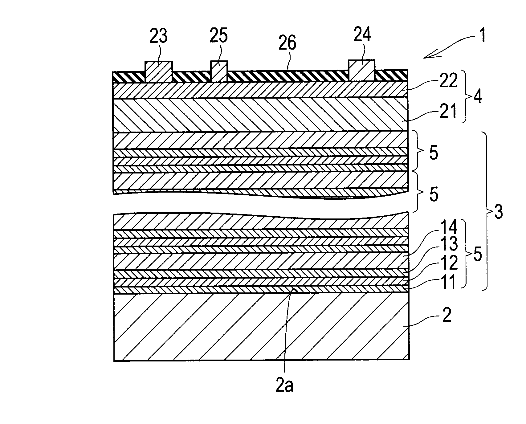
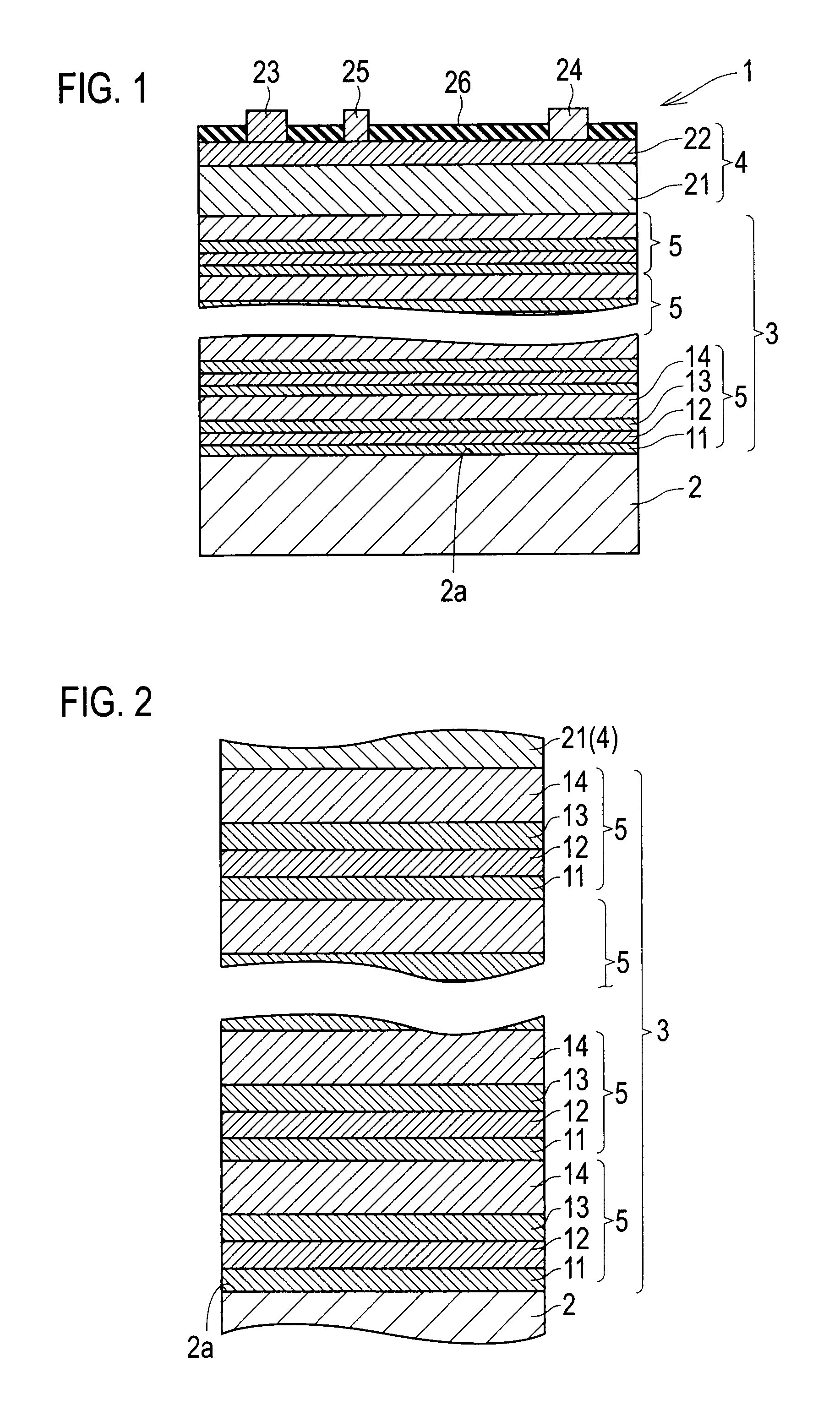
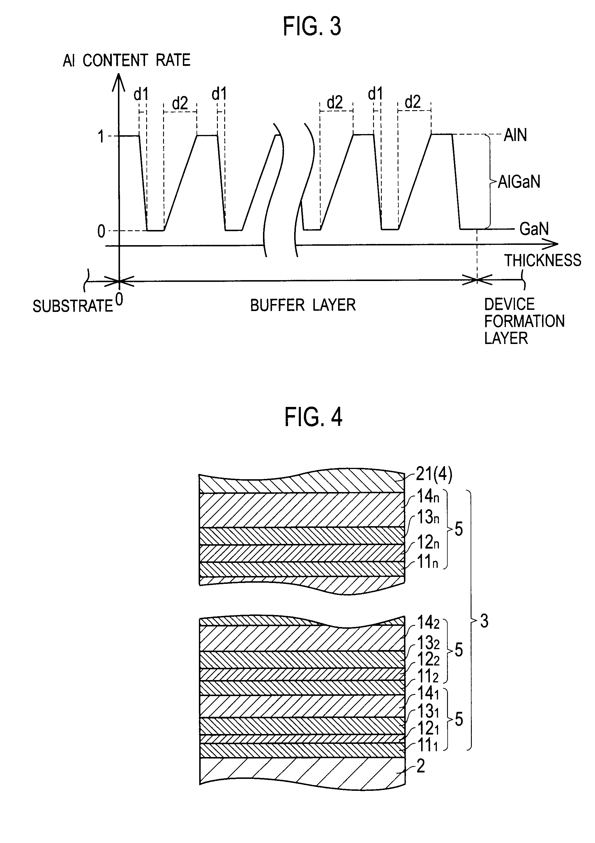
[0027]A first embodiment in which a semiconductor device according to the present invention is applied to an HEMT (high electron mobility transistor) is described with reference to the drawings. FIG. 1 is a cross-sectional view of the semiconductor device according to the first embodiment. FIG. 2 is a cross-sectional view of a buffer layer. FIG. 3 is a graph showing a relationship between thicknesses of constituent layers of the buffer layer and Al content rates of the constituent layers.

[0028]As shown in FIG. 1, a semiconductor device 1 according to the first embodiment includes a substrate 2, a buffer layer 3, and a device formation layer 4.

[0029]The substrate 2 supports the buffer layer 3 and the device formation layer 4. The substrate 2 is made of n-type monocrystalline silicon containing n-type impurities of a group V element such as P (phosphorus).

[0030]The buffer layer 3 functions to relax a stress resulting from a difference in lattice constant between silicon constituting t...

second embodiment

[0065]A second embodiment in which a buffer layer differs from the buffer layer according to the first embodiment is described next. FIG. 4 is a cross-sectional view of the buffer layer according to the second embodiment. FIG. 5 is a graph showing a relationship between thicknesses of constituent layers of the buffer layer and Al content rates of the constituent layers. Like constituent elements as those according to the first embodiment are denoted by like reference signs and descriptions thereof will be omitted.

[0066]As shown in FIGS. 4 and 5, in the buffer layer 3 according to the second embodiment, thicknesses d1m and d2m of first and second composition graded layers 12m and 14m closer to the substrate 2 are smaller than thicknesses d1m and d2m of first and second composition graded layers 12m and 14m closer to the device formation layer 4, respectively. It is assumed that m=1, 2, . . . n.

[0067]That is, the first and second composition graded layers 12m, and 14m are formed so th...

third embodiment

[0072]A third embodiment in which a buffer layer differs from those according to the above embodiments is described next. FIG. 6 is a graph showing a relationship between thicknesses of constituent layers of the buffer layer according to the third embodiment and Al content rates of the constituent layers. Like constituent elements as those according to the above embodiments are denoted by like reference signs and descriptions thereof will be omitted.

[0073]As shown in FIG. 6, in the buffer layer 3 according to the second embodiment, thicknesses d1m and d2m of first and second composition graded layers 12m and 14m closer to the substrate 2 are larger than thicknesses d1m and d2m of first and second composition graded layers 12m and 14m closer to the device formation layer 4, respectively.

[0074]That is, the first and second composition graded layers 12m and 14m are formed so that the thicknesses d1m and d2m satisfy, respectively:

[0075]d11>d12> . . . >d1n, and

[0076]d21>d22> . . . >d2n. ...


PUM


Abstract

A device includes a substrate; a buffer layer; and a device formation layer, wherein the buffer layer is formed by sequentially stacking, a plurality of times, a first nitride-based semiconductor layer made of a material having a lattice constant lower than a lattice constant of a material of the substrate; a first composition graded layer made of a material having a lattice constant gradually higher than the lattice constant of the first nitride-based semiconductor layer in a thickness direction; a second nitride-based semiconductor layer made of a material having a lattice constant higher than the lattice constant of the first nitride-based semiconductor layer; and a second composition graded layer made of a material having a lattice constant gradually lower than the lattice constant of the second nitride-based semiconductor layer in the thickness direction, and the second composition graded layer is thicker than the first composition graded layer.

Description

CROSS REFERENCE TO RELATED APPLICATIONS AND INCORPORATION BY REFERENCE[0001]This application is based upon and claims the benefit of priority from prior Japanese Patent Application P2009-076235 filed on Mar. 26, 2009; the entire contents of which are incorporated by reference herein.TECHNICAL FIELD[0002]The present invention relates to a semiconductor device constituted by a substrate and a device formation layer made of different materials.BACKGROUND ART[0003]When a device formation layer made of a different semiconductor material from that of a substrate is to be formed on the substrate, damage such as cracks disadvantageously occurs due to a difference in lattice constant between the substrate and the device formation layer.[0004]Considering this problem, Patent Literature 1 discloses a technique for suppressing damage such as cracks. According to this conventional technique, a buffer layer is provided between a substrate and a device formation layer. The buffer layer includes a ...

Claims


Application Information

Patent Timeline
Patent Type & Authority Applications(United States)
IPC IPC(8): H01L29/205
CPCH01L21/02381H01L21/02458H01L21/02505H01L21/02507H01L21/0254H01L29/7787H01L29/1075H01L29/2003H01L29/205H01L29/7783H01L21/0262
Inventor SATO, KEN
Owner SANKEN ELECTRIC CO LTD
Why Eureka
Try Eureka