
Data processing device and data processing system

a data processing device and data processing technology, applied in transmission systems, physical parameter compensation/prevention, instruments, etc., can solve problems such as inability to ensure data continuity, and achieve the effect of ensuring data continuity

Active Publication Date: 2010-09-30
RENESAS ELECTRONICS CORP
View PDF3 Cites 9 Cited by
  • Summary
  • Abstract
  • Description
  • Claims
  • Application Information

AI Technical Summary

Benefits of technology

The present invention provides an arrangement for ensuring data continuity in the conversion of a voltage under measurement, using an amplifier circuit and an AD converter circuit. This is achieved by directly converting the analog signal after amplification and calculating the gain and offset of the amplifier circuit. By canceling the gain error through a ratio of expected gain to the calculated gain, data continuity can be ensured between the result of conversion after amplification and the result of direct conversion without using the amplifier circuit. This technique does not require error calibration of the amplifier circuit and ensures higher precision in conversion.

Problems solved by technology

This conventional practice is, however, disadvantageous in that data continuity may not be ensured between the result of conversion after amplification by using the amplifier circuit and the result of direct conversion without using the amplifier circuit.
A gain error and offset of the amplifier circuit are the causes of the disadvantageous phenomenon mentioned above.

Method used


Image

  • Data processing device and data processing system
  • Data processing device and data processing system
  • Data processing device and data processing system

Examples


Embodiment Construction

1. Overviews of the Preferred Embodiments

[0038]First, the present invention will be described below regarding the overviews of representative preferred embodiments thereof. It is to be noted that, in the following description of the overviews of the representative preferred embodiments, parenthesized reference numerals are used for illustrative purposes only and designate respective parts that are included in the concepts of corresponding component elements identified with reference numerals in the accompanying drawings.

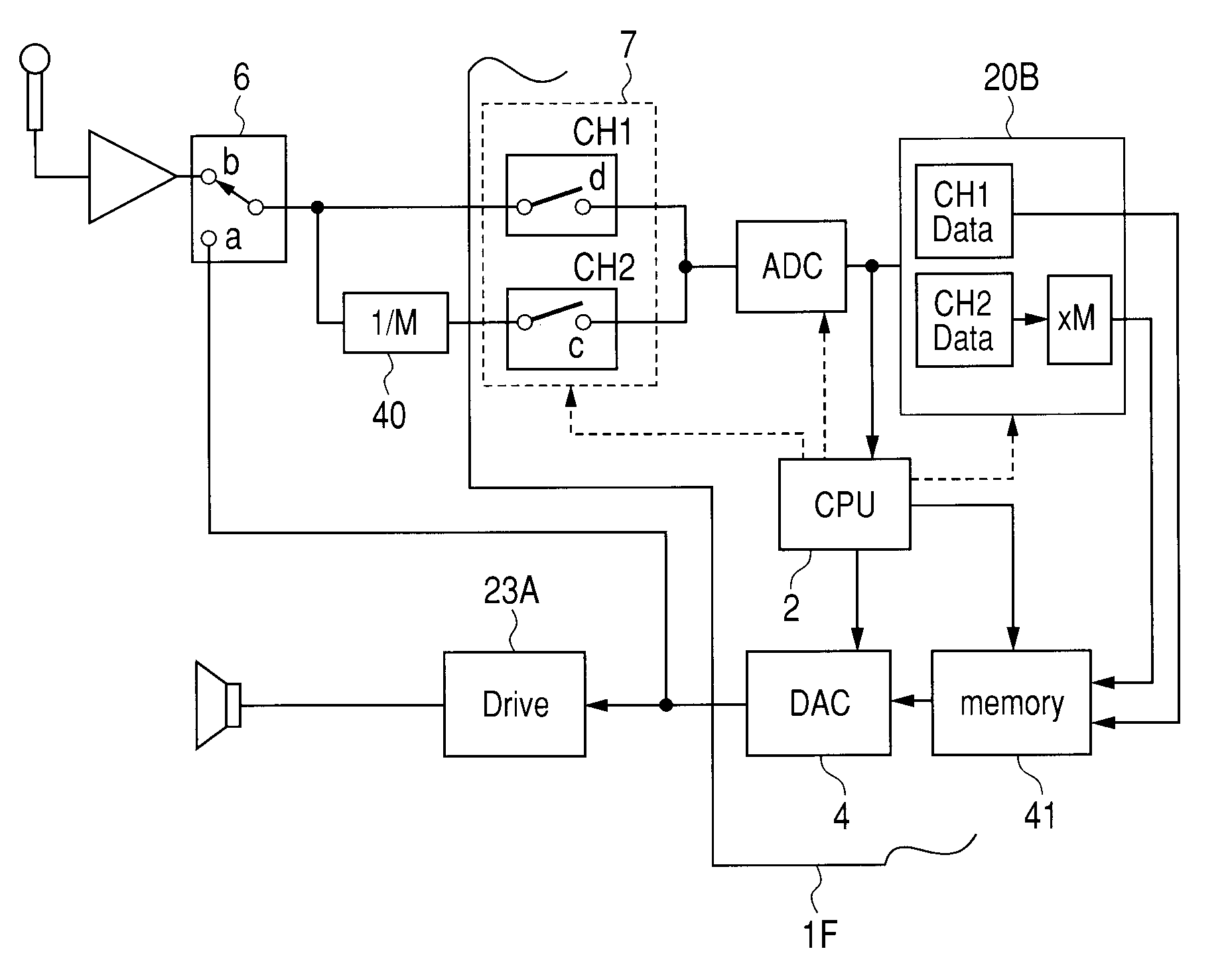
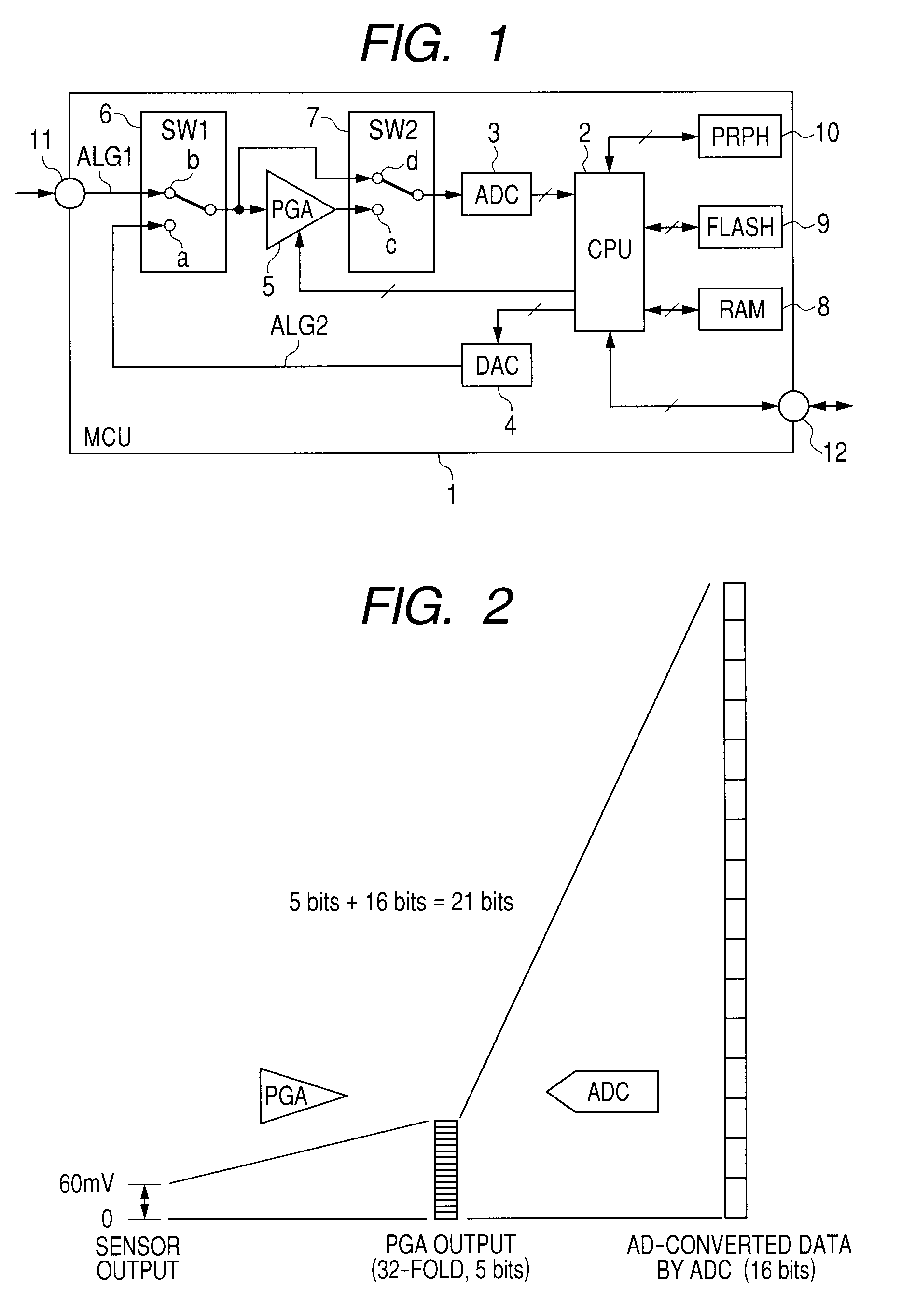
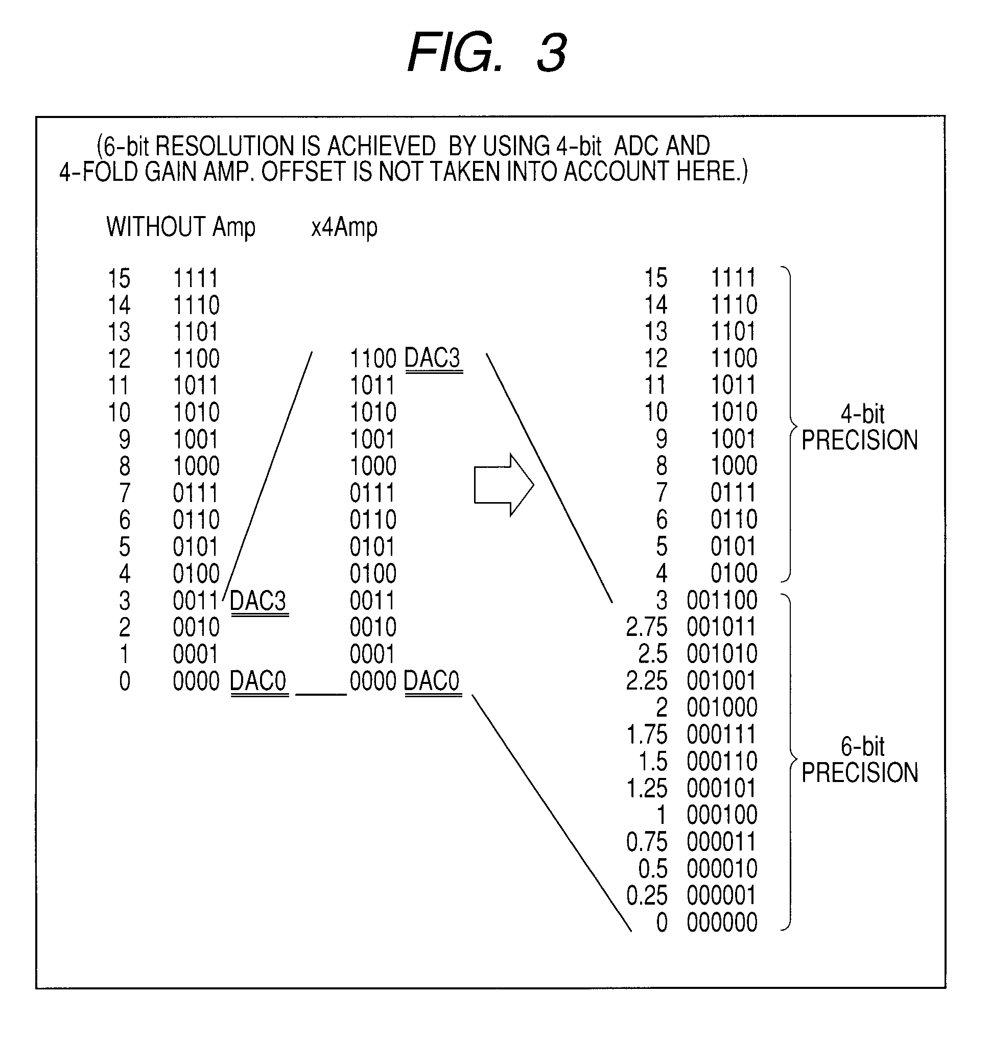
[1] According to one representative preferred embodiment of the present invention, a data processing device (1) comprises a DA converter circuit (4), an amplifier circuit (5), an AD converter circuit (3), and a control circuit (2). The control circuit is so designed as to control calibration processing and bit-precision-variable AD conversion processing for the amplifier circuit with an expected gain of 2n (“n” represents a positive integer). In execution of the cali...


PUM


Abstract

In AD conversion of a voltage under measurement, data continuity is ensured between the result of conversion after amplification by using an amplifier circuit and the result of direct conversion without using the amplifier circuit. In AD conversion operation using a DA converter circuit, an amplifier circuit, and an AD converter circuit under the direction of a control circuit, an analog signal output from the DA converter circuit is directly converted by the AD converter circuit, and also the analog signal is converted therein after amplified by the amplifier circuit with an expected gain of 2n (“n” represents a positive integer). Based on resultant data thus obtained, a gain of the amplifier circuit and an offset thereof are calculated. An analog signal under measurement to be enhanced in bit precision is subjected to amplification by the amplifier circuit and conversion by the AD converter circuit, the offset calculated as mentioned above is subtracted from the result of the conversion, and the result of the subtraction thus performed is multiplied by a ratio of the expected gain to the gain calculated as mentioned above so as to cancel a gain error. Then, based on data with the gain error canceled, acquisition of bit-extended conversion result data is performed to ensure continuity between data having different degrees of bit precision.

Description

CROSS-REFERENCE TO RELATED APPLICATIONS[0001]The disclosure of Japanese Patent Application No. 2009-84822 filed on Mar. 31, 2009 and Japanese Patent Application No. 2009-223765 filed on Sep. 29, 2009 each including the specification, drawings and abstract are incorporated herein by reference in its entirety.BACKGROUND OF THE INVENTION[0002]The present invention relates to a data processing device having an analog-to-digital (AD) conversion function, and more particularly to a technique for enhancing the degree of conversion bit precision (resolution) in small-signal operation with respect to an AD conversion range.[0003]In Patent Documents 1 and 2 indicated below, there are disclosed techniques for acquiring AD conversion result data having a higher degree of bit precision than that of an AD converter circuit.[0004]According to the Patent Document 1, an AD converter device is so arranged that an input voltage is compared with a voltage obtained through DA conversion of AD-converted ...

Claims


Application Information

Patent Timeline
Patent Type & Authority Applications(United States)
IPC IPC(8): H03M1/10
CPCH03M1/1028H03M1/12H03M1/1009H03M1/183
Inventor ISO, YOSHIMIKIMURA, KAKERUMATSUSHIMA, TADASHISHIMIZU, YUJI
Owner RENESAS ELECTRONICS CORP
Learn More