

Miniature image capture lens
- Summary
- Abstract
- Description
- Claims
- Application Information
AI Technical Summary
Benefits of technology
Problems solved by technology
Method used
Image

Examples
first embodiment
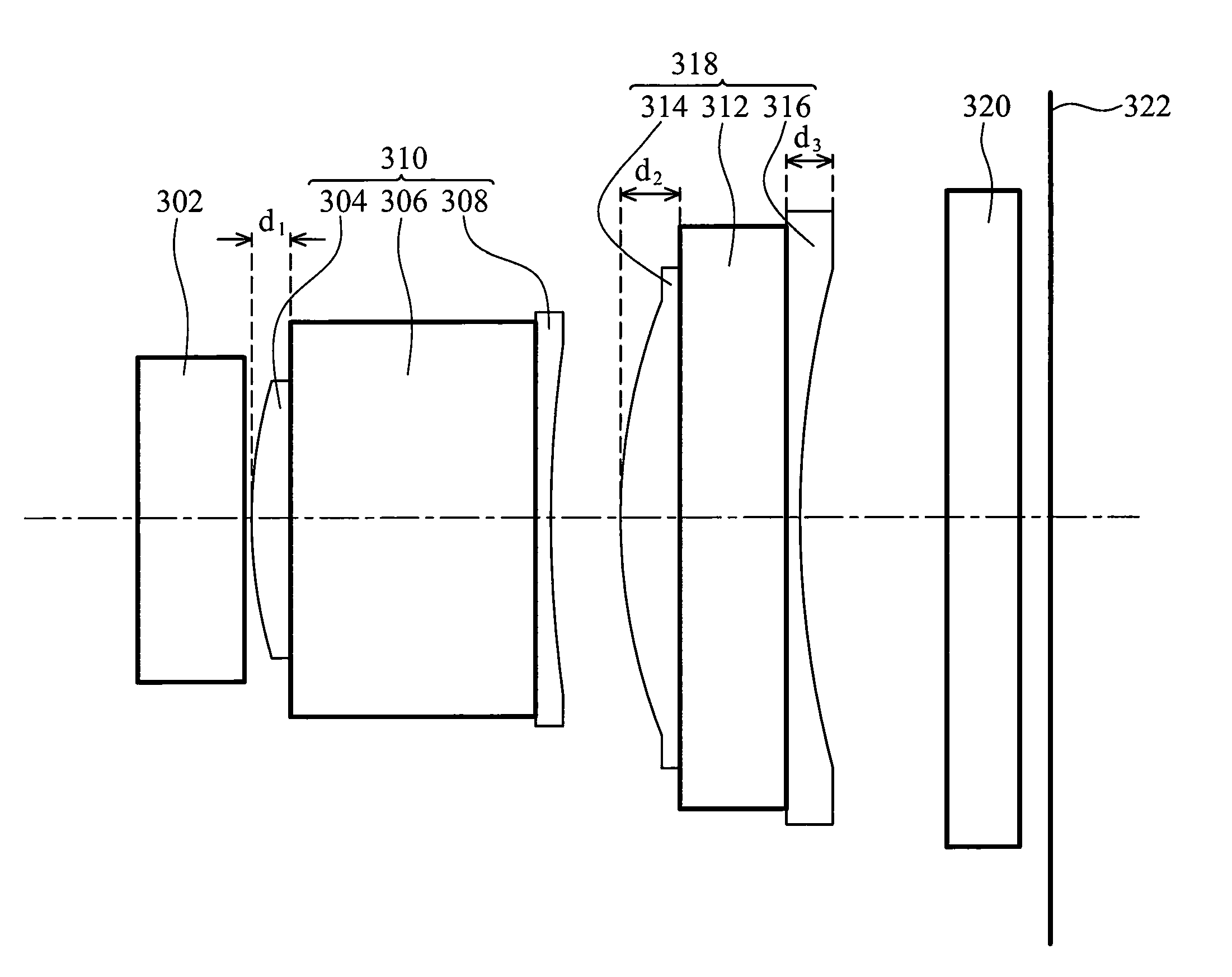
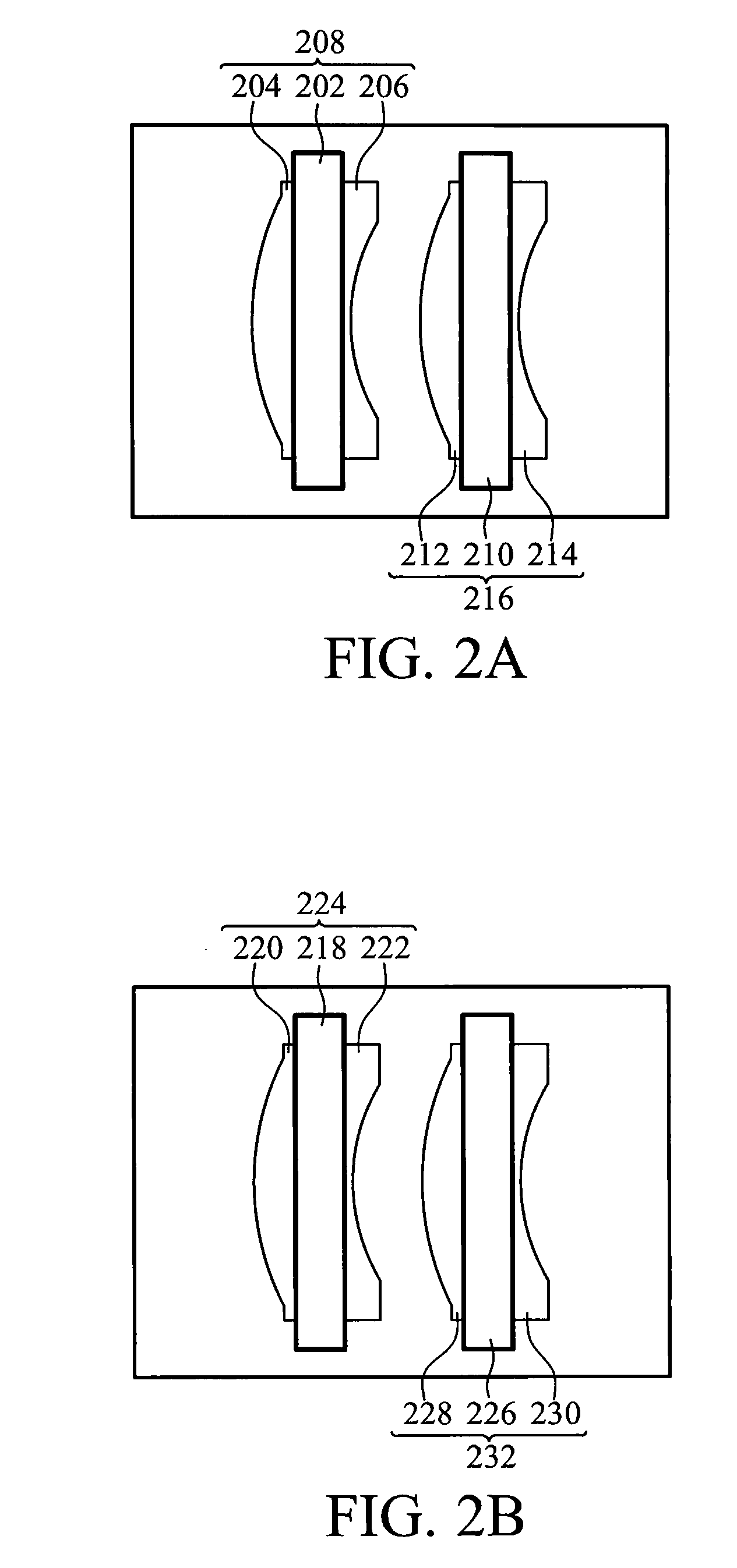
[0031]Referring to FIG. 2A, which shows a lens design of the invention, a first substrate 202 and a second substrate 210 are provided, and a first surface 204 is disposed on the first side of the first substrate 202, a second surface 206 is disposed on a second side of the first substrate 202 to constitute a first lens group 208, a third surface 212 is disposed on the first side of the second substrate 210, and a fourth surface 214 is disposed on the second side of the second substrate 210 to constitute a second lens group 216. In the embodiment, the first surface 204 has high refraction index Nd_h, high abbe number Vd_h and convex shaped (positive curvature), the second surface 206 has low refraction index Nd_l, low abbe number Vd_l and concave shaped (negative curvature), the third surface 212 has high refraction index Nd_h, high abbe number Vd_h and convex shaped (positive curvature), and the fourth surface 214 has low refraction index Nd_l, low abbe number Vd_l and concave shape...
second embodiment
[0032]Referring to FIG. 2B, which shows a lens design of the invention, a first substrate 218 and a second substrate 226 are provided, and a first surface 220 is disposed on the first side of the first substrate 218, a second surface 222 is disposed on a second side of the first substrate 218 to constitute a first lens group 224, a third surface 228 is disposed on the first side of the second substrate 226, and a fourth surface 230 is disposed on the second side of the second substrate 226 to constitute a second lens group 232. In the embodiment, the first surface 220 has low refraction index Nd_l, low abbe number Vd_l and convex shaped (positive curvature), the second surface 222 has high refraction index Nd_h, high abbe number Vd_h and concave shaped (negative curvature), the third surface 228 has low refraction index Nd_l, low abbe number Vd_l and convex shaped (positive curvature), and the fourth surface 230 has high refraction index Nd_h, high abbe number Vd_h and concave shape...
third embodiment
[0033]Referring to FIG. 2C, which shows a lens design of the invention, a first substrate 234 and a second substrate 242 are provided, and a first surface 236 is disposed on the first side of the first substrate 234, a second surface 238 is disposed on a second side of the first substrate 234 to constitute a first lens group 240, a third surface 244 is disposed on the first side of the second substrate 242, and a fourth surface 246 is disposed on the second side of the second substrate 242 to constitute a second lens group 248. In the embodiment, the first surface 236 has high refraction index Nd_h, high abbe number Vd_h and convex shaped (positive curvature), the second surface 238 has low refraction index Nd_l, low abbe number Vd_l and concave shaped (negative curvature), the third surface 244 has low refraction index Nd_l, low abbe number Vd_l and concave shaped (negative curvature), and the fourth surface 246 has high refraction index Nd_h, high abbe number Vd_h and convex shape...
PUM
 Abstract
Description
Claims
Application Information