

Method for fabricating semiconductor device using a double patterning process
- Summary
- Abstract
- Description
- Claims
- Application Information
AI Technical Summary
Benefits of technology
Problems solved by technology
Method used
Image

Examples
Embodiment Construction
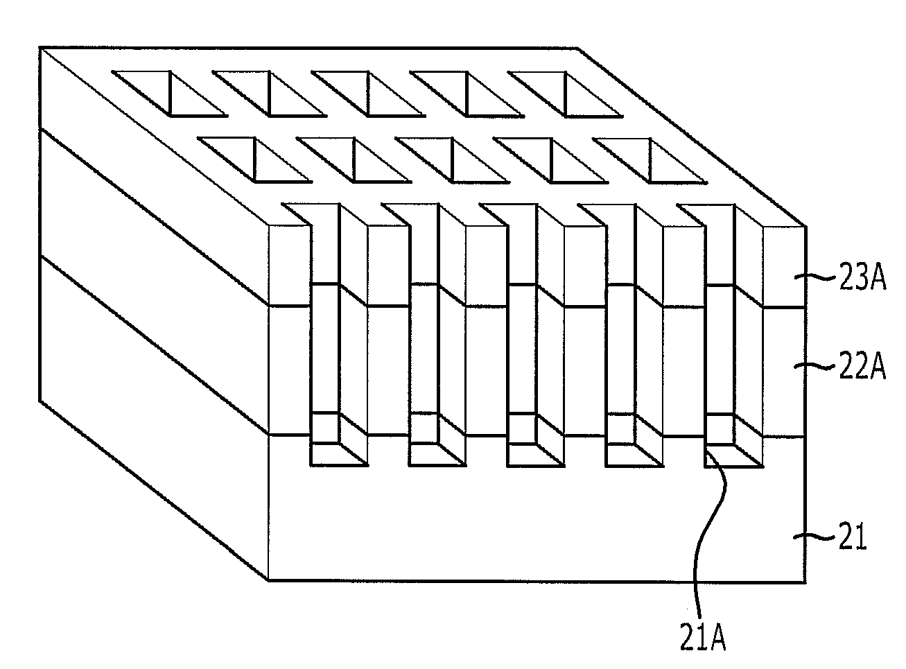
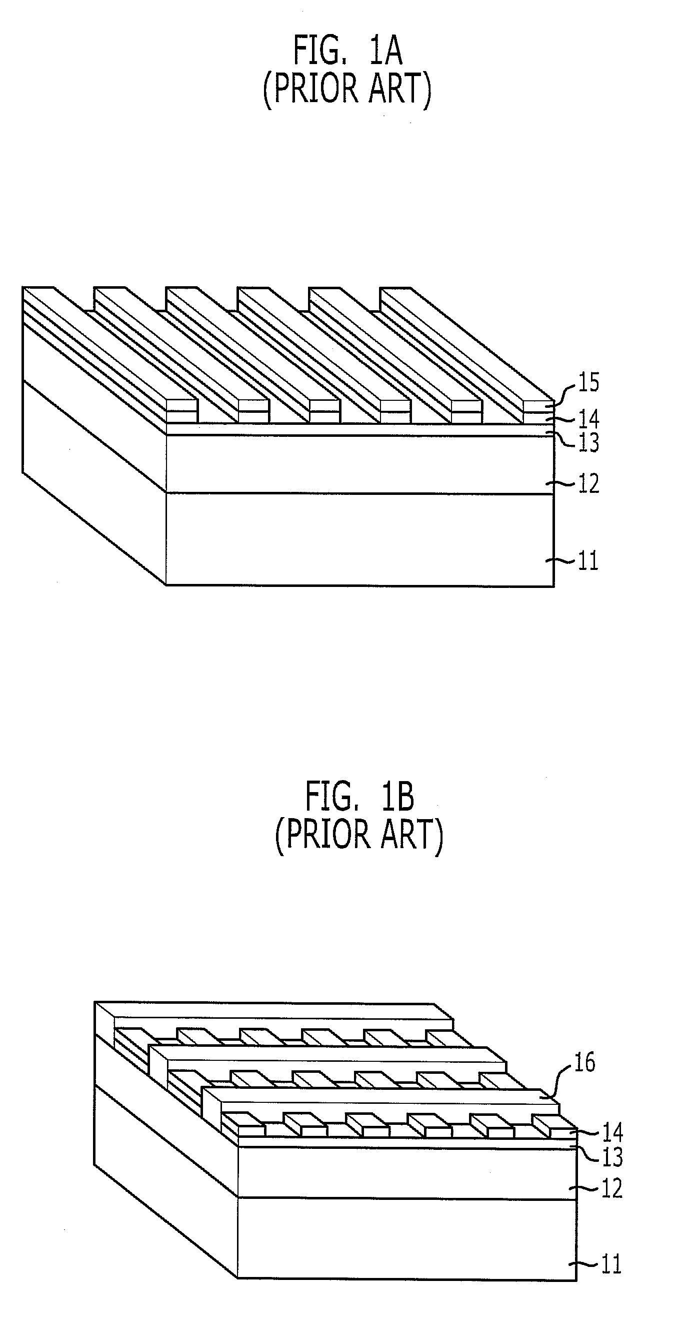
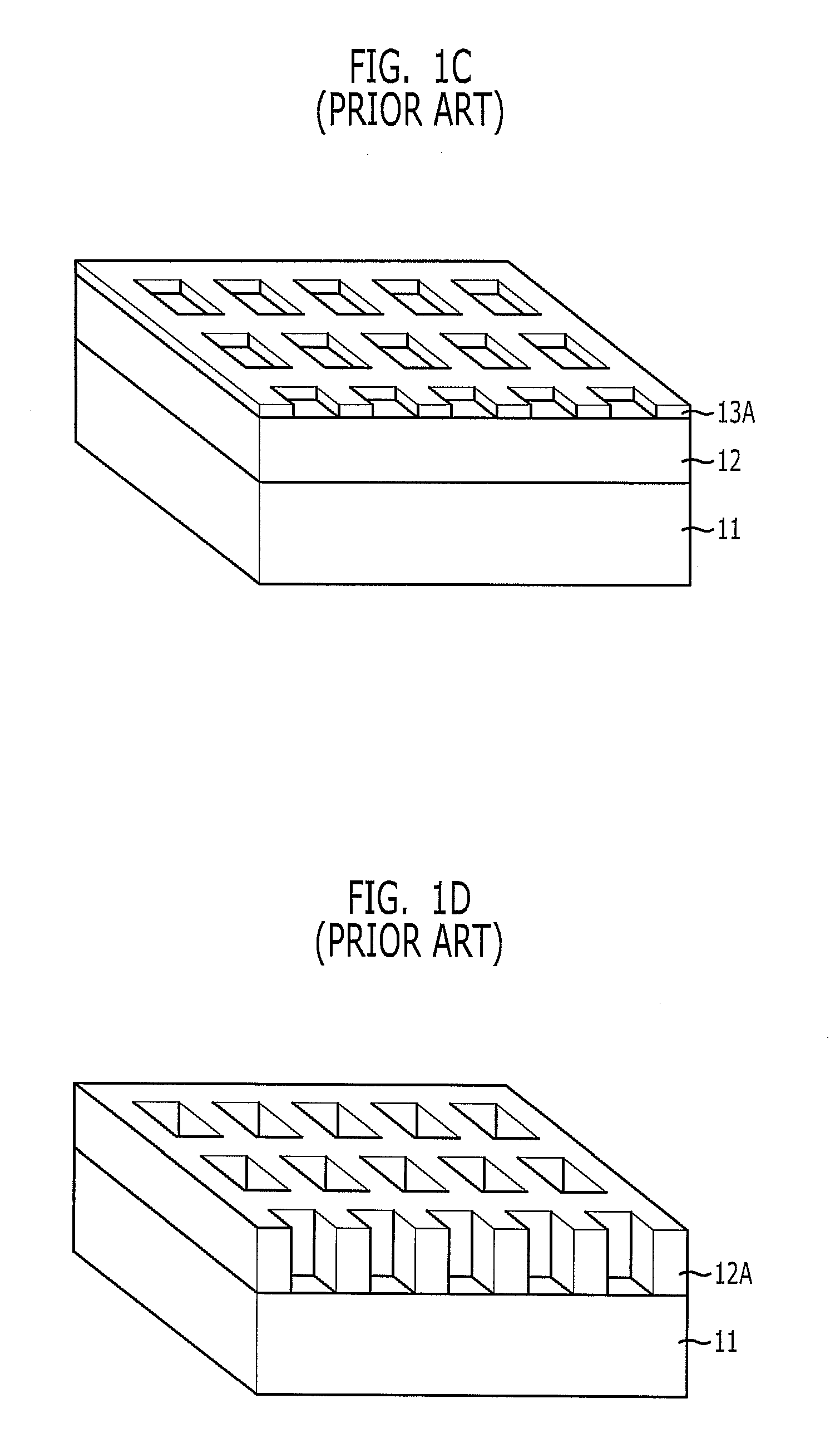
[0030]Hereinafter, a method for fabricating a micropattern of a semiconductor device in accordance with the present invention will be described in detail with reference to the accompanying drawings. In the drawings, the thicknesses of layers and regions are exemplary and may not be exact. It will be understood that when an element such as a layer, a film, a pattern and a region is referred to as being “on / under” another element herein, it may be directly on / under the other element, and one or more intervening elements may also be present. Like reference numerals in the drawings denote like elements throughout the drawings. In addition, changes to the reference numerals of layers by, for example, addition of letters, refer to a partial deformation of the layers by an etch process or a polishing process.
[0031]Embodiments of the present invention use a triple hard mask as a hard mask instead of using a double hard mask while a double patterning process is performed. The triple hard mas...
PUM
| Property | Measurement | Unit |
|---|---|---|
| Power | aaaaa | aaaaa |
| Power | aaaaa | aaaaa |
| Angle | aaaaa | aaaaa |
Abstract
Description
Claims
Application Information