Light emitting apparatus, electronic equipment and method of driving pixel circuit

a technology of light emitting apparatus and electronic equipment, which is applied in the direction of instruments, light sources, computing, etc., can solve the problem of instantaneous cause of unsatisfactory light emission, and achieve the effect of suppressing light emission

Active Publication Date: 2010-10-07
SEIKO EPSON CORP
View PDF9 Cites 26 Cited by
  • Summary
  • Abstract
  • Description
  • Claims
  • Application Information

AI Technical Summary

Benefits of technology

[0007]An advantage of some aspects of the invention is to suppress light emission of a light emitting device due to charges left on a node between a driving transistor and a light emission control transistor.
[0009]According to the configuration, in the discharge period provided immediately before the light emission period, the light emission control transistor and the discharge transistor are set to be in the ON-state. Therefore, charges left between the driving transistor and the light emission control transistor when the writing of the data potential is completed can be sufficiently removed. Accordingly, an advantage that light emission of the light emitting device due to the charges left between the driving transistor and the light emission control transistor can be suppressed is obtained.
[0012]With this configuration, charges accumulated in the node due to the compensation operation and the writing of the data potential, for example, are discharged to the electric supply line through the discharge transistor. That is to say, there is an advantage that the charges left in the node between the driving transistor and the light emission control transistor can be surely removed before the light emission period is started.
[0014]With this configuration, since a circuit for generating a control signal controlling the ON- and OFF-states of the light emission control transistor needs not be separately provided, the configuration thereof can be simplified. For example, when a plurality of pixel circuits are arranged in a matrix form, a signal controlling ON- and OFF-states of the second switching devices and the light emission control transistors in the pixel circuits of each row is generally generated by using a shift register. With the above configuration, a signal controlling the ON- and OFF-states of the light emission control transistor is generated by inverting and delaying the control signal controlling ON- and OFF-states of the second switching device. Therefore, an advantage that a shift register for generating a signal controlling the ON- and OFF states of the light emission control transistor needs not be separately provided is obtained.

Problems solved by technology

This causes a problem that undesired light emission is instantaneously caused.

Method used


Image

  • Light emitting apparatus, electronic equipment and method of driving pixel circuit
  • Light emitting apparatus, electronic equipment and method of driving pixel circuit
  • Light emitting apparatus, electronic equipment and method of driving pixel circuit

Examples


modification 1

(1) Modification 1

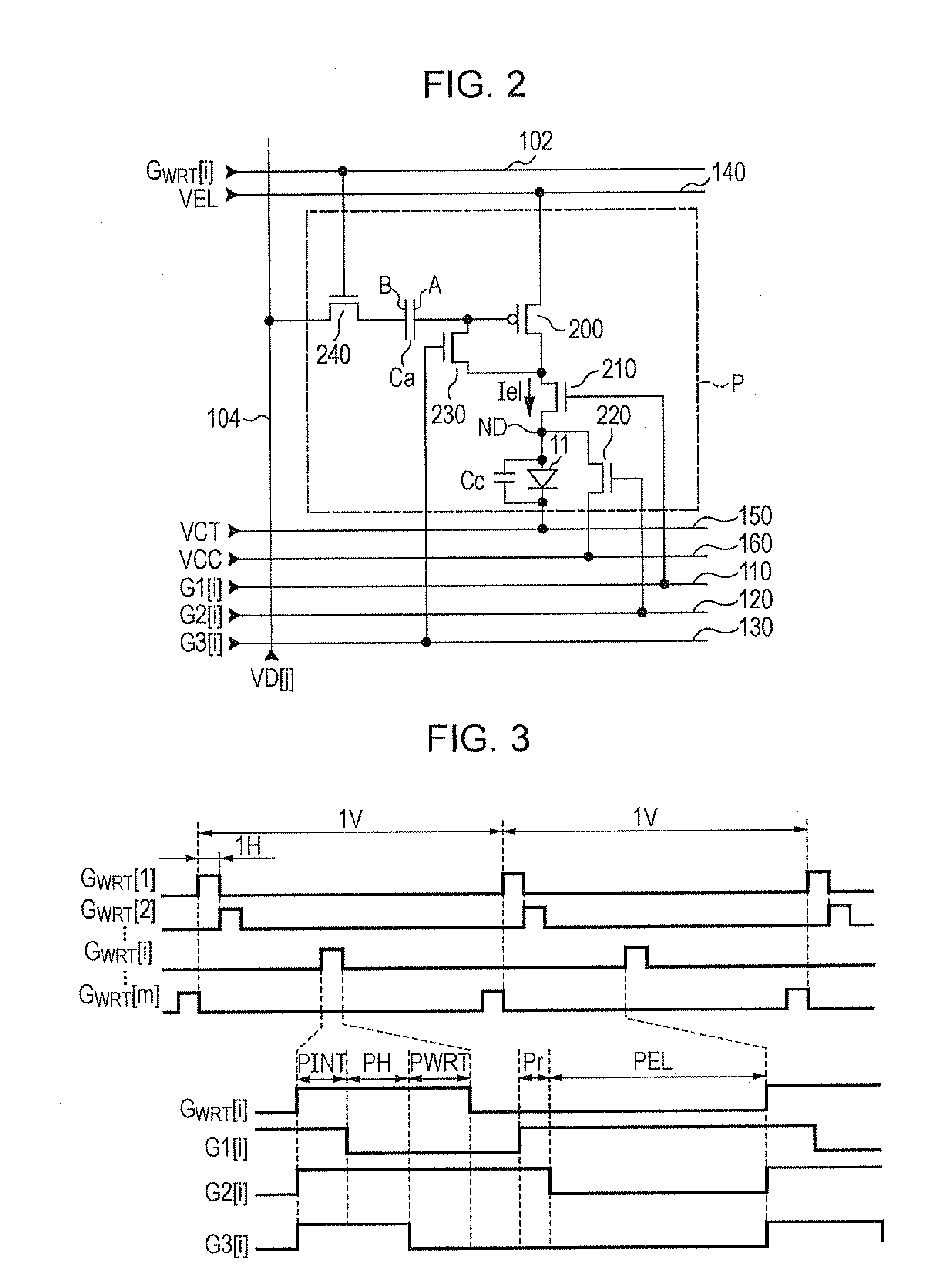
[0070]As shown in FIG. 12, the third power supply line 160 can be eliminated. In a configuration shown in FIG. 12, the source of the discharge transistor 220 is connected to the second power supply line 150. The configuration shown in FIG. 12 has an advantage that the number of the power supply lines can be reduced in comparison with that in the above embodiment of the invention. However, it is to be noted that the potential of the node ND when the discharge transistor 220 is in the ON-state is lower than a potential which is higher than the potential VCT by the threshold voltage of the light emitting device 11 in the configuration shown in FIG. 12.

modification 2

(2) Modification 2

[0071]Although the discharge transistor 220 is an N-channel type in the above embodiment of the invention, the discharge transistor 220 is not limited thereto and may be a P-channel type. However, according to a mode in which the discharge transistor 220 is configured as the N-channel type, the potential supplied to the gate of the discharge transistor 220 when the discharge transistor 220 is in the ON-state can be lower in comparison with a mode in which the discharge transistor 220 is configured as the P-channel type. Accordingly, there is an advantage that when the discharge transistor 220 is in the OFF-state, an amount of leakage current generated on the discharge transistor 220 can be reduced.

modification 3

(3) Modification 3

[0072]As shown in FIG. 13, a third switching device 250 may be provided between a fourth power supply line to which the potential VST is supplied and the second electrode B. A gate of the third switching device 250 is connected to a fourth control line 180 to which a fourth control signal G4[i] is supplied. In a mode shown in FIG. 13, the scan line driving circuit 20 sets the scan signal GWRT[i] to high level only in the writing period PWRT, and sets the scan signal GWRT[i] to low level in the initialization period PINT and the compensation period PH. On the other hand, the scan line driving circuit 20 sets the fourth control signal G4[i] to high level in the initialization period PINT and the compensation period PH, and sets the fourth control signal G4[i] to low level in other periods. Accordingly, the third switching device 250 is set to be in the ON-state in the initialization period PINT and the compensation period PH so that the second electrode B is conducte...


PUM


Abstract

A light emitting apparatus includes a pixel circuit and a driving circuit which drives the pixel circuit. The pixel circuit includes: a driving transistor which generates a driving current; a light emitting device that determines gradation depending on the driving current; a light emission control transistor; a discharge transistor; a capacitor device; and a first switching device interposed between a gate and a drain of the driving transistor.

Description

BACKGROUND[0001]1. Technical Field[0002]The present invention relates to a light emitting apparatus, electronic equipment and a method of driving a pixel circuit.[0003]2. Related Art[0004]In recent years, an organic light emitting diode device (hereinafter, referred to as “OLED device”) which is also referred to as an electroluminescent (EL) device or a light emitting polymer device attracts attention as a next-generation light emitting device alternative to a liquid crystal device. Gradation (typically, brightness) of the light emitting device of this type changes when an electric current is supplied to the light emitting device. A configuration in which the current is controlled by a driving transistor has been proposed hitherto.[0005]A pixel circuit of the light emitting apparatus disclosed in Japanese Patent No. 4,131,227 includes a light emission control transistor between the driving transistor and the OLED device. Further, the pixel circuit disclosed in Japanese Patent No. 4,...

Claims


Application Information

Patent Timeline
Patent Type & Authority Applications(United States)
IPC IPC(8): G09G5/00
CPCH05B37/02G09G3/3233G09G2300/0819G09G2320/045G09G2310/0251G09G2310/0262G09G2320/043G09G2300/0842H05B47/10
Inventor YAMAMOTO, GAKUJI
Owner SEIKO EPSON CORP
Why Eureka
Try Eureka