Silicon-based dielectric stack passivation of si-epitaxial thin-film solar cells

a silicon-based dielectric and thin-film technology, applied in the field of solar cell manufacturing, can solve the problems of increasing the manufacture cost of solar cells, and reducing the efficiency of solar cells

Active Publication Date: 2010-10-14
SOLARCITY
View PDF6 Cites 20 Cited by
  • Summary
  • Abstract
  • Description
  • Claims
  • Application Information

AI Technical Summary

Problems solved by technology

The negative environmental impact caused by the use of fossil fuels and their rising cost have resulted in a dire need for cleaner, cheaper alternative energy sources.
For homojunction solar cells, minority-carrier recombination at the cell surface due to the existence of defect states and dangling bonds can significantly reduce the solar cell efficiency; thus, a good surface passivation process is needed.
Due to the soaring cost of Si material, the existence of such a thick crystalline-Si substrate significantly increases the manufacture cost of solar cells; therefore, solar cells based on thin-film technology have been gaining popularity.

Method used


Image

  • Silicon-based dielectric stack passivation of si-epitaxial thin-film solar cells
  • Silicon-based dielectric stack passivation of si-epitaxial thin-film solar cells
  • Silicon-based dielectric stack passivation of si-epitaxial thin-film solar cells

Examples


Embodiment Construction

[0026]The following description is presented to enable any person skilled in the art to make and use the embodiments, and is provided in the context of a particular application and its requirements. Various modifications to the disclosed embodiments will be readily apparent to those skilled in the art, and the general principles defined herein may be applied to other embodiments and applications without departing from the spirit and scope of the present disclosure. Thus, the present invention is not limited to the embodiments shown, but is to be accorded the widest scope consistent with the principles and features disclosed herein.

Overview

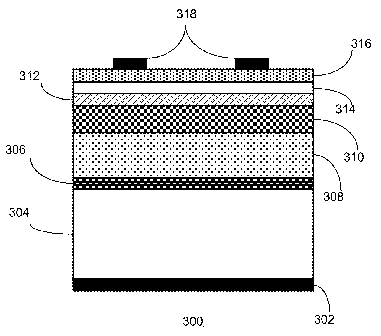
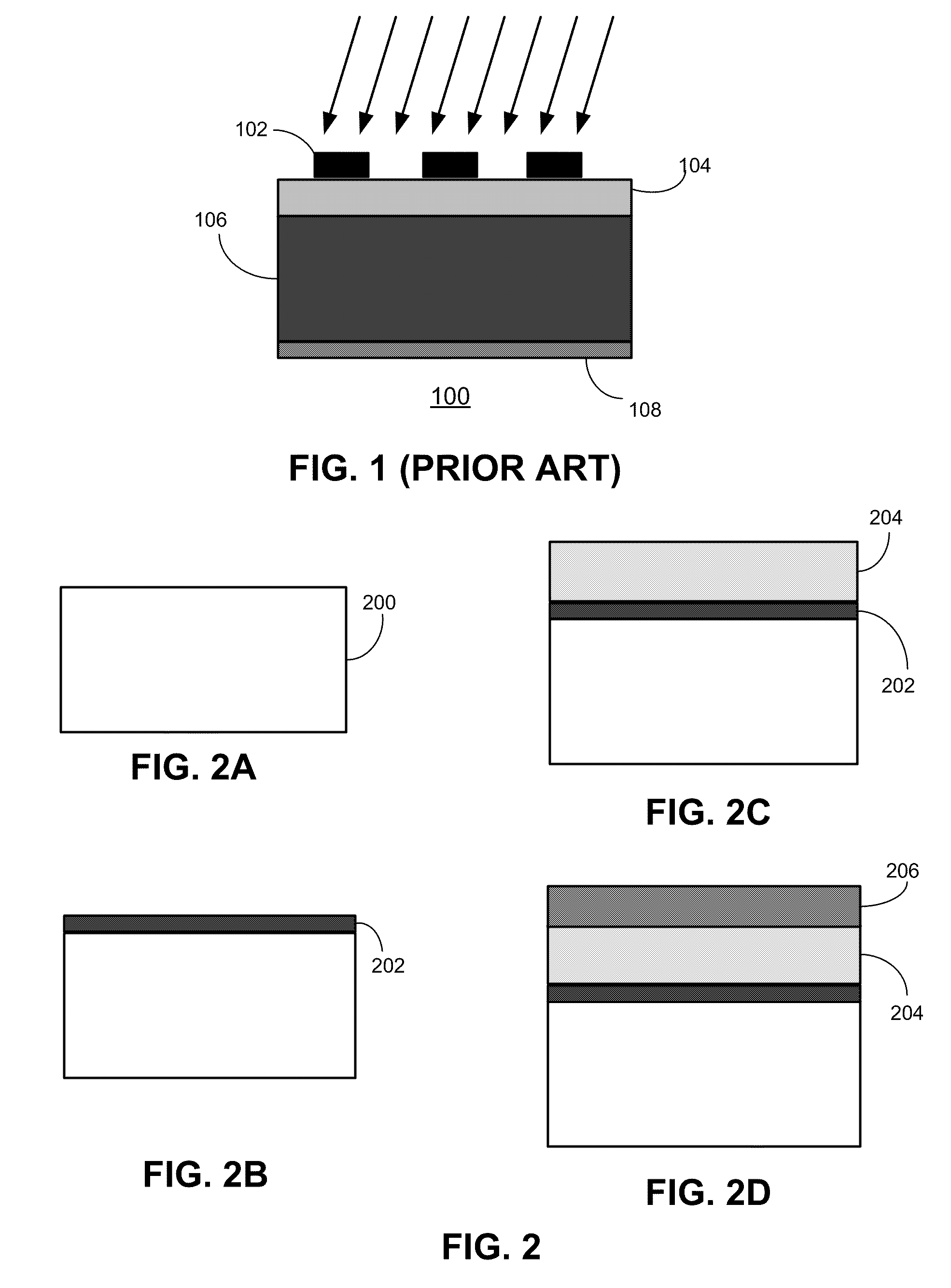
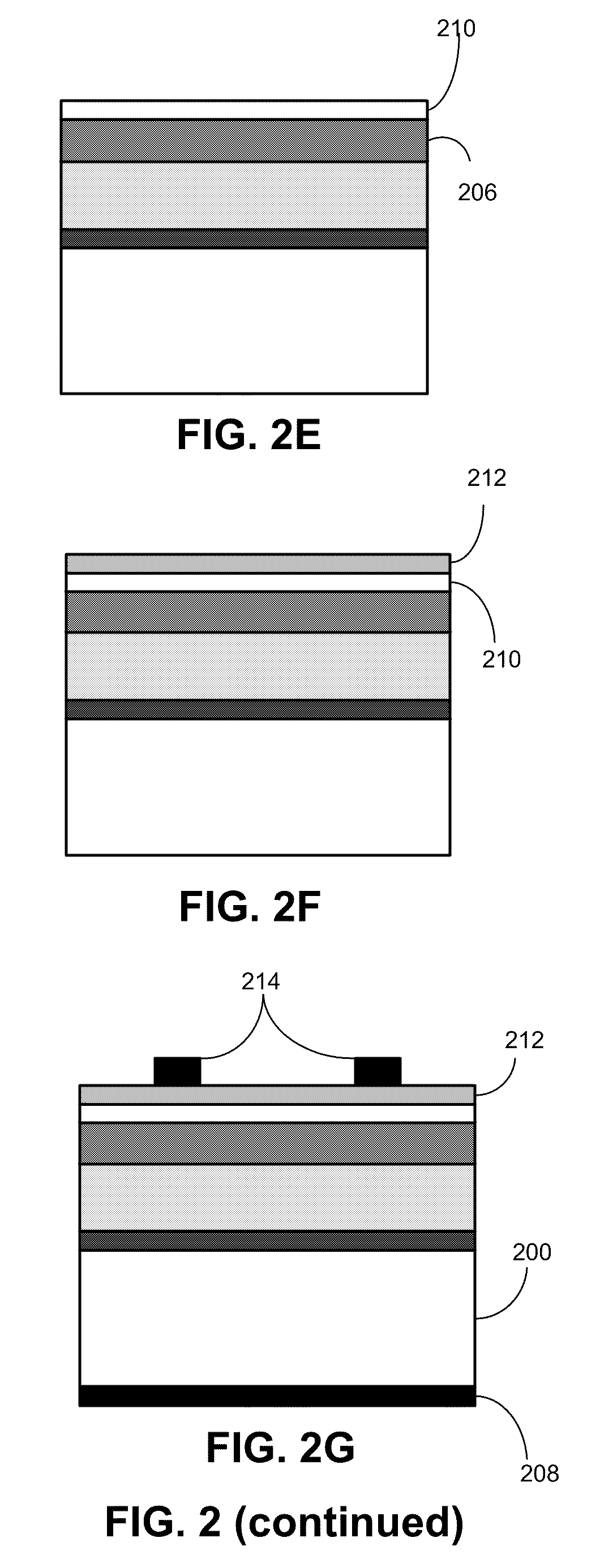
[0027]Embodiments of the present invention provide a solar cell using a two / three-layer dielectric stack for passivation and anti-reflection. A thin layer of heavily p-type doped crystalline-Si is deposited on a metallurgical-grade Si (MG-Si) substrate forming a back-surface-field (BSF) layer, and a thin layer of lightly p-type doped crystalline-Si...


PUM


Abstract

One embodiment of the present invention provides a solar cell. The solar cell includes a metallurgical-grade Si (MG-Si) substrate, a first layer of heavily doped crystalline-Si situated above the MG-Si substrate, a layer of lightly doped crystalline-Si situated above the first heavily doped crystalline-Si layer, a backside ohmic-contact layer situated on the backside of the MG-Si substrate, a second layer of heavily doped crystalline-Si situated above the lightly doped crystalline-Si layer, a first layer of dielectric situated above the second heavily doped crystalline-Si layer, a second layer of dielectric situated above the first dielectric layer, and front electrodes situated above the second dielectric layer.

Description

BACKGROUND[0001]1. Field[0002]This disclosure is generally related to manufacturing a solar cell. More specifically, this disclosure is related to integrating a silicon-based dielectric stack for surface and bulk passivation with screen-printing technology for a Si-epitaxial thin-film solar cell manufacturing application.[0003]2. Related Art[0004]The negative environmental impact caused by the use of fossil fuels and their rising cost have resulted in a dire need for cleaner, cheaper alternative energy sources. Among different forms of alternative energy sources, solar power has been favored for its cleanness and wide availability.[0005]A solar cell converts light into electricity using the photoelectric effect. There are several basic solar cell structures, including a single p-n junction, p-i-n / n-i-p, and multi-junction. A typical single p-n junction structure includes a p-type doped layer and an n-type doped layer. Solar cells with a single p-n junction can be homojunction solar ...

Claims


Application Information

Patent Timeline
Patent Type & Authority Applications(United States)
IPC IPC(8): H01L31/00H01L31/18
CPCH01L31/02167H01L31/02168Y02E10/547H01L31/068H01L31/1804H01L31/022425Y02P70/50
Inventor YU, CHENTAOFU, JIANMINGHENG, JIUNN BENJAMIN
Owner SOLARCITY
Why Eureka
Try Eureka