Liquid crystal display device

Active Publication Date: 2010-10-14
PANASONIC LIQUID CRYSTAL DISPLAY CO LTD +1
View PDF3 Cites 7 Cited by
  • Summary
  • Abstract
  • Description
  • Claims
  • Application Information

AI Technical Summary

Benefits of technology

[0013]In this case, the above-mentioned image sticking may be reduced by employing the structure described in JP 2007-183299 A cited above. However, the degree of irregularity due to a level difference between the surface of the common electrode and the surfaces of the pixel electrodes is increased to impair flatness of the surfaces on the liquid crystal LC side. As a result, the irregularity is reflected

Problems solved by technology

However, in the liquid crystal display device illustrated in FIG. 4, it is found that charges are likely to accumulate in the capacitor insulator CI so as to disadvantageously cause so-called image sticking.
The DC current is accumulated in the capacitor insulator CI and changes the voltage applied to the liquid crystal LC, thereby causing the image sticking as a change in brightness dependent on a drive voltage.
As a result, there is a problem that the image sticking becomes noticeable.
As a result, there is a problem of occurrence of a phenomenon called “f

Method used


Image

  • Liquid crystal display device
  • Liquid crystal display device
  • Liquid crystal display device

Examples


Example

First Embodiment

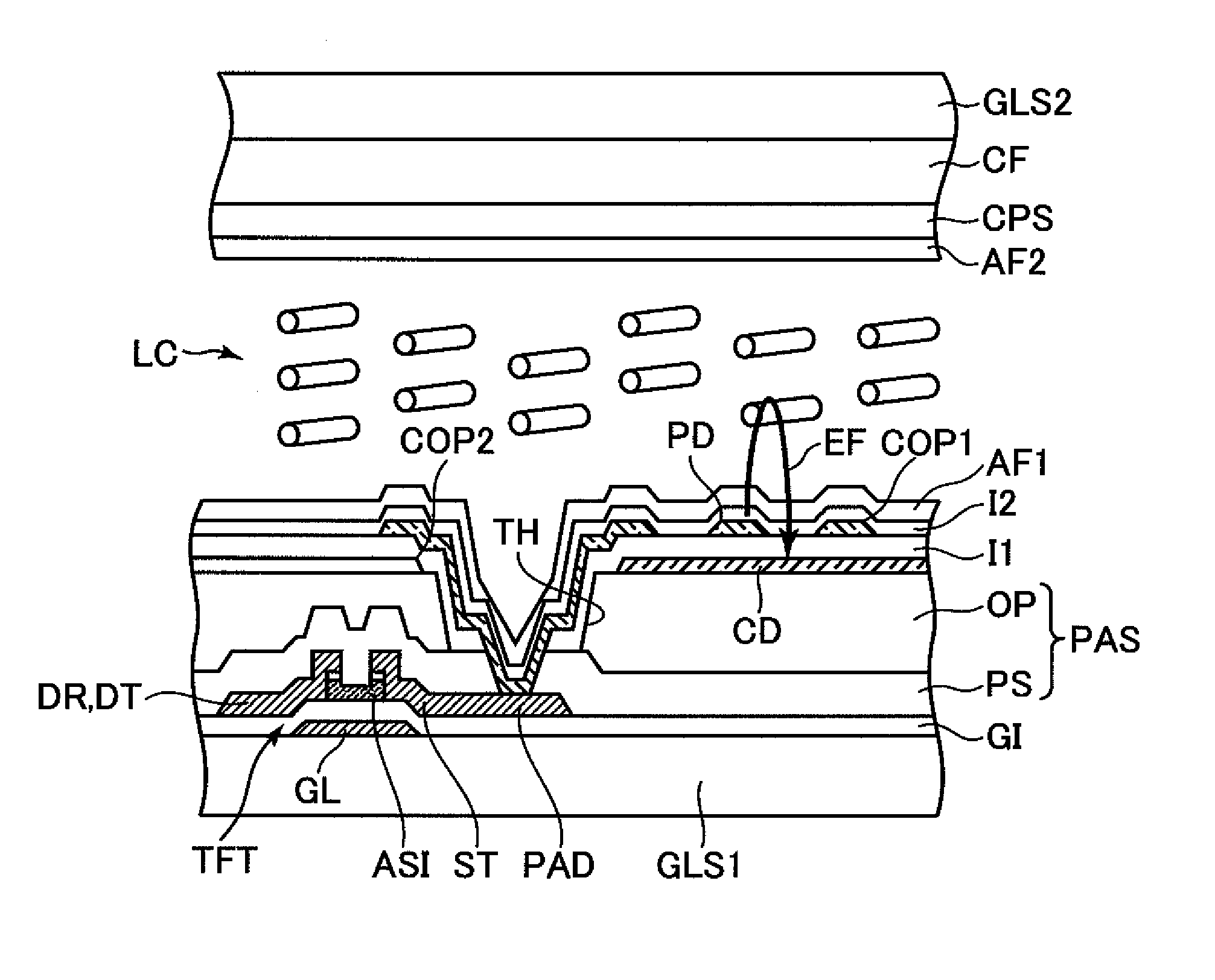
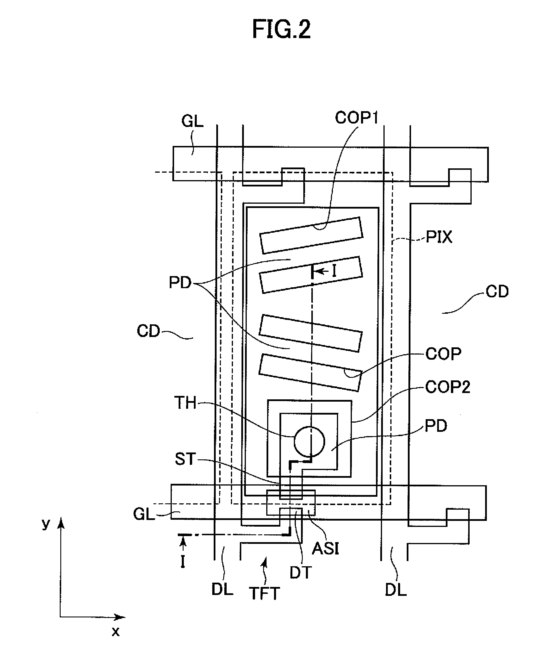
[0038]FIG. 2 is a view illustrating a structure of a pixel, which illustrates a first embodiment of a liquid crystal display device of the present invention. FIG. 2 is a plan view as viewed from a liquid crystal side of one substrate GLS1 of a pair of substrates GLS1 and GLS2 which are provided so as to be opposed to each other with a liquid crystal LC interposed therebetween. FIG. 1 is a sectional view taken along a line I-I illustrated in FIG. 2. FIG. 1 also illustrates another substrate GLS2 which is provided so as to be opposed to the substrate GLS1 with the liquid crystal LC interposed therebetween.

[0039]First, as illustrated in FIG. 2, a pair of neighboring gate bus lines GL, each extending in an x-direction of FIG. 2, are arranged in parallel in a y-direction. A pair of neighboring data bus lines DL, each extending in the y-direction, are arranged in parallel in the x-direction. A region surrounded by the pair of gate bus lines GL and the pair of data bus line...

Example

Second Embodiment

[0051]FIG. 6 is a view illustrating a structure of the pixel, illustrating a second embodiment of the liquid crystal display device of the present invention. FIG. 7 is a sectional view taken along a line VII-VII illustrated in FIG. 6.

[0052]FIG. 6 is depicted for the comparison with FIG. 2. Differences between the structure illustrated in FIG. 6 and that in FIG. 2 are as follows. First, the thin film transistor TFT includes a semiconductor layer made of polycrystalline silicon PSI. Further, the thin film transistor TFT is a so-called double-gate thin film transistor having two gates. Moreover, the pixel electrodes PD have a comb-like pattern obtained by arranging a plurality of (for example, three in FIG. 6) of linear electrodes, each extending in the y-direction of FIG. 6, in parallel in the x-direction. Further, the common electrode CD is connected to the common electrode CD of the neighboring pixel in the x-direction of FIG. 6 over the data bus line DL. In this m...

Example

Third Embodiment

[0058]FIG. 8 is a view illustrating a structure of the pixel, illustrating a third embodiment of the liquid crystal display device of the present invention. FIG. 9 is a sectional view taken along a line IX-IX illustrated in FIG. 8.

[0059]FIG. 8 is depicted for the comparison with FIG. 2. Differences between the structure illustrated in FIG. 8 and the structure illustrated in FIG. 2 are as follows. First, regarding the common electrodes CD and the pixel electrode PD formed as different layers through the insulator, the pixel electrode PD is located below, whereas the common electrodes CD are located above. In this case, the pixel electrode PD is formed of a sheet-like electrode made of, for example, ITO, which is provided in the region where the pixel PIX is formed. On the other hand, the common electrodes CD are formed by forming holes COP3 through, for example, an ITO film which is formed over the entire liquid crystal display area (the ITO film is formed even in a ...


PUM


Abstract

A liquid crystal display device includes a first substrate and a second substrate. The first substrate includes a sheet-like first electrode formed of a transparent conductive film, a first insulator formed to cover the sheet-like first electrode, a plurality of linear second electrodes formed by a transparent conductive film on the first insulator so as to overlap the sheet-like first electrode, and a second insulator formed on the first insulator so as to cover the plurality of linear second electrodes. The first substrate and the second substrate interpose liquid crystal therebetween and are arranged to be opposed to each other. The sheet-like first electrode, the first insulator, and the plurality of linear second electrodes are provided in a pixel region on a surface of the first substrate of a side of the liquid crystal. The second insulator is made of the same material as the first insulator.

Description

CROSS-REFERENCE TO RELATED APPLICATION[0001]The present application claims priority from Japanese Applications JP 2009-094004 filed on Apr. 8, 2009, the content to which is hereby incorporated by reference into this application.BACKGROUND OF THE INVENTION[0002]1. Field of the Invention[0003]The present invention relates to a liquid crystal display device, in particular, to an in plane switching liquid crystal display device having a structure called fringe field switching (FFS).[0004]2. Description of the Related Art[0005]A cross section of a pixel structure of an in plane switching liquid crystal display device having a structure called fringe field switching (FFS) is illustrated in FIG. 4. FIG. 4 is depicted for comparison with FIG. 1 which illustrates an embodiment of the present invention. Therefore, for a detailed structure of FIG. 4 other than the parts described below, see the description given for FIG. 1.[0006]As illustrated in FIG. 4, a thin film transistor TFT, pixel elect...

Claims


Application Information

Patent Timeline
IPC IPC(8): G02F1/1333
CPCG02F1/133345G02F2001/134372G02F1/134363G02F1/134372
Inventor SATO, TAKESHIOKA, SHINICHIROTOYOTA, YOSHIAKI
Owner PANASONIC LIQUID CRYSTAL DISPLAY CO LTD
Why Eureka
Try Eureka