

Clock data recovery circuit and multiplied-frequency clock generation circuit
a clock data and clock generation technology, applied in the field of clock data recovery, can solve the problem of no longer being able to set the band width, and achieve the effect of preventing the probability of erroneous reception from increasing and preventing the reception margin
- Summary
- Abstract
- Description
- Claims
- Application Information
AI Technical Summary
Benefits of technology
Problems solved by technology
Method used
Image

Examples
first embodiment
1: First Embodiment Implementing a First Typical Configuration of the CDR Circuit
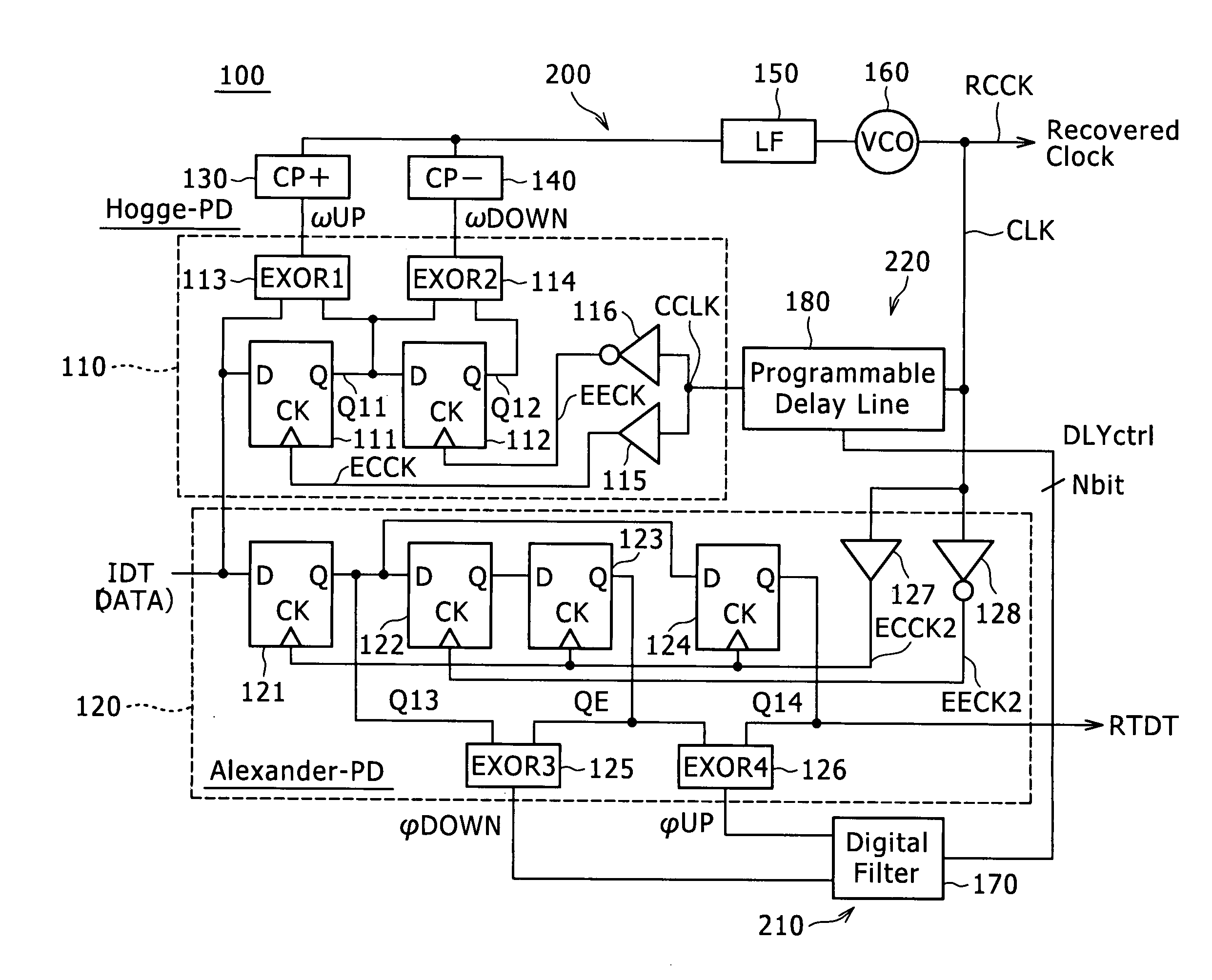
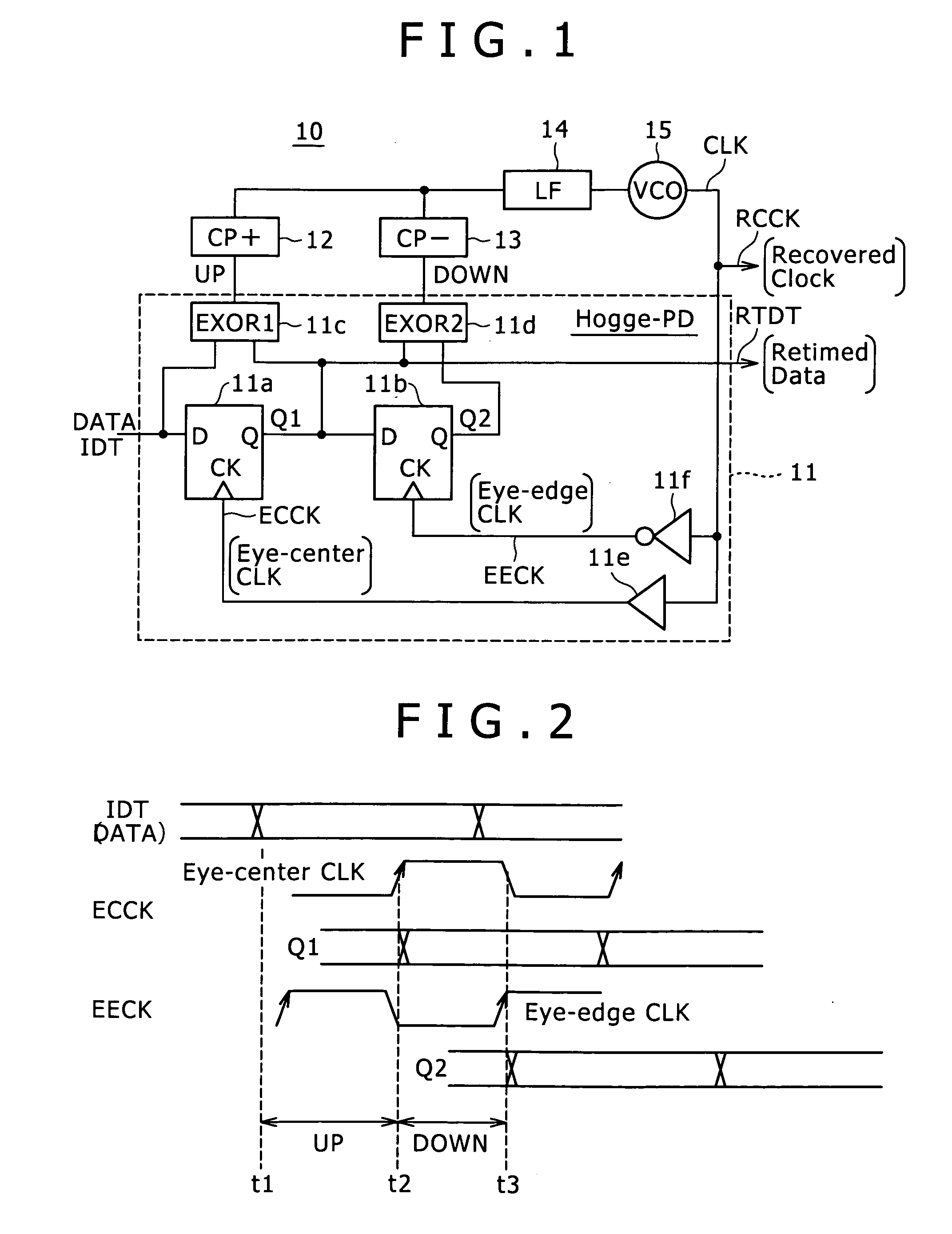
[0079]FIG. 9 is a block diagram showing the configuration of a CDR circuit 100 according to a first embodiment of the present invention.
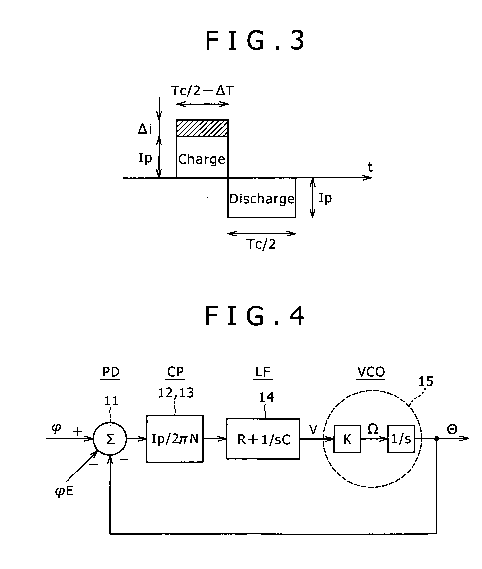
[0080]As shown in the block diagram of FIG. 9, the CDR circuit 100 according to the first embodiment employs a first phase detector 110, a second phase detector 120, a first charge pump (CP+) 130, a second charge pump (CP−) 140, an LF (Loop Filter) 150 and a VCO (Voltage-Controlled Oscillator) 160.
[0081]In addition, the CDR circuit 100 also has a digital filter 170 and a programmable delay line 180.
[0082]The first phase detector 110 is a Hogge phase detector whereas the second phase detector 120 is an Alexander phase detector. Thus, the CDR circuit 100 according to the first embodiment has a hybrid phase detector which is implemented by the first phase detector 110 and the second phase detector 120.
[0083]Basically, the CDR circuit 100 according to the first embodiment i...
second embodiment
2: Second Embodiment Implementing a Second Typical Configuration of the CDR Circuit
[0155]FIG. 13 is a block diagram showing the configuration of a CDR circuit 100A according to a second embodiment of the present invention.
[0156]Differences between the CDR circuit 100A according to the second embodiment and the CDR circuit 100 according to the first embodiment are explained as follows.
[0157]In place of the digital filter 170 supposed to be used as a phase correction information generation section 210A for the CDR circuit 100A, a third charge pump (φCP+) 211, a fourth charge pump (φCP−) 212 and a filter capacitor (Cφ) 213 are employed in the CDR circuit 100A.
[0158]In addition, in place of the programmable delay line 180 supposed to be used as a phase correction information addition section 220A for the CDR circuit 100A, a current feedback section 221 is employed in the CDR circuit 100A.
[0159]On top of that, the second phase detector 120A employed in the CDR circuit 100A does not have ...
third embodiment
3: Third Embodiment Implementing a Third Typical Configuration of the CDR Circuit
[0170]FIG. 15 is a block diagram showing the configuration of a CDR circuit 100B according to a third embodiment of the present invention.
[0171]The CDR circuit 100B according to the third embodiment has differences from the CDR circuit 100 according to the first embodiment and the CDR circuit 100A according to the second embodiment as explained below.
[0172]The VCO employed in the CDR circuit 100B according to the third embodiment is a multi-phase VCO 160B for generating four clock signals CKa, CKb, CKy and CKz which have phases shifted from each other by an angle of 90 degrees. In addition, the CDR circuit 100B employs a modified second phase detector 300 associated with the multi-phase VCO 160B as a substitute for the second phase detector 120A.
[0173]In the case of the third embodiment, the frequency of the clock signals CKa, CKb, CKy and CKz generated by the multi-phase VCO 160B is half of the frequen...
PUM
 Abstract
Description
Claims
Application Information