Check patentability & draft patents in minutes with Patsnap Eureka AI!

Non-volatile semiconductor memory circuit for generating write voltage

a non-volatile, memory circuit technology, applied in static storage, digital storage, instruments, etc., can solve the problems of large footprint and complicated circuit structur

Active Publication Date: 2010-10-21
SK HYNIX INC
View PDF11 Cites 3 Cited by
  • Summary
  • Abstract
  • Description
  • Claims
  • Application Information

AI Technical Summary

Benefits of technology

[0011]According to another aspect, a non-volatile semiconductor memory circuit includes a memory cell array, a write controller configured to repeatedly verify and determine whether input data is written down in the memory cell array to write the input data in

Problems solved by technology

Therefore, since the PRAM needs the circuit for selecting the data input and output mode and separate controllers in the standby state and an active state (where the pumps are required to be driven), a large footprint is needed and the structure of the circuits is complicated.

Method used


Image

  • Non-volatile semiconductor memory circuit for generating write voltage
  • Non-volatile semiconductor memory circuit for generating write voltage
  • Non-volatile semiconductor memory circuit for generating write voltage

Examples


Embodiment Construction

.”

BRIEF DESCRIPTION OF THE DRAWINGS

[0014]The above and other aspects, features and other advantages of the subject matter of the present disclosure will be more clearly understood from the following detailed description taken in conjunction with the accompanying drawings, in which:

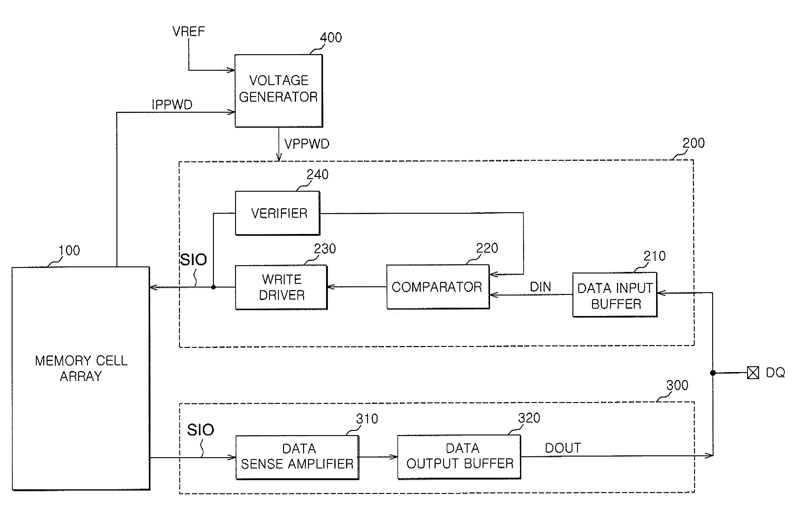
[0015]FIG. 1 is a block diagram of a structure of an example of a non-volatile semiconductor memory circuit according to one embodiment;

[0016]FIG. 2 is a block diagram showing a structure of an example of a voltage generator illustrated in FIG. 1;

[0017]FIG. 3 is a block diagram showing a structure of an example of a control signal generator illustrated in FIG. 2;

[0018]FIG. 4 is a block diagram showing a structure of an example of a first control signal generator illustrated in FIG. 3;

[0019]FIG. 5 is a circuit diagram showing a structure of an example of a control voltage generator illustrated in FIG. 2; and

[0020]FIG. 6 is a voltage waveform showing relationships between a write voltage and a first control ...


PUM


Abstract

A non-volatile semiconductor memory circuit for generating a write voltage is presented. The non-volatile semiconductor memory circuit includes a memory cell and a voltage generator. The voltage generator provides a write voltage at a given target level that varies in accordance with an amount of current detected by the memory cell array by using a reference voltage.

Description

CROSS-REFERENCES TO RELATED APPLICATION[0001]The present application claims priority under 35 U.S.C. 119(a) to Korean application number 10-2009-0032671, filed on Apr. 15, 2009, in the Korean Intellectual Property Office, which is incorporated by reference in its entirety as if set forth in full.BACKGROUND OF THE INVENTION[0002]1. Technical Field[0003]The present invention described herein relates to a non-volatile semiconductor memory circuit and, more particularly, to a non-volatile semiconductor memory circuit for generating a write voltage.[0004]2. Related Art[0005]Generally, a phase change random access memory (PRAM) tends to be researched and developed to be adopted to various semiconductor systems and semiconductor memory devices due to a characteristic in that it is common that the PRAM can randomly access data although the PRAM is a non-volatile memory.[0006]A unit cell of the PRAM often times includes a diode, for example, one switching element connected to a word line and...

Claims


Application Information

Patent Timeline
IPC IPC(8): G11C11/00G11C5/14G11C7/00
CPCG11C5/143G11C13/0038G11C13/0004G11C5/145G11C16/30G11C16/34
Inventor SHIN, YOON JAE
Owner SK HYNIX INC
Features
  • R&D
  • Intellectual Property
  • Life Sciences
  • Materials
  • Tech Scout
  • Unparalleled Data Quality
  • Higher Quality Content
  • 60% Fewer Hallucinations
Learn More