
Eureka
For R&D, Eureka makes reading and utilizing patents & technical documents easy.
Eureka AIR
Designed for self-driven R&D workflows. Generate viable solutions, solve complex R&D challenges, empower your innovation with AI.

Eureka Materials
Designed for material experts only. Revolutionize your material R&D, from search, analyze, to developing new materials.

TechResearch
Generate reliable direction feasibility study reports for your R&D in just a few steps.

TechSeek
Discover and master advanced knowledge NOW. Basics, ideas, possibilities, all at once.

TechMind
As an expert in R&D Theories, TechMind can generates customized viable solutions instantly.

TechRisk
Analyze your overall solution with one click, know your potential R&D risks in advance.

TechMonitor
Get weekly tech updates, stay abreast of the latest tech innovations and key insights.
Method of manufacturing semiconductor device
- Summary
- Abstract
- Description
- Claims
- Application Information
AI Technical Summary
Problems solved by technology
Method used
Image

Examples
Embodiment Construction
[0017]Exemplary embodiments of method of manufacturing semiconductor device according to the present invention will be explained below in detail with reference to the accompanying drawings. The present invention is not limited to the following embodiments.
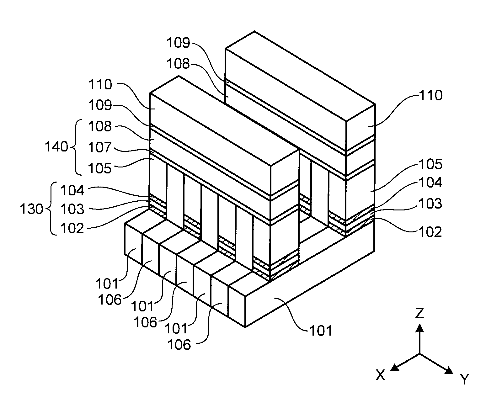
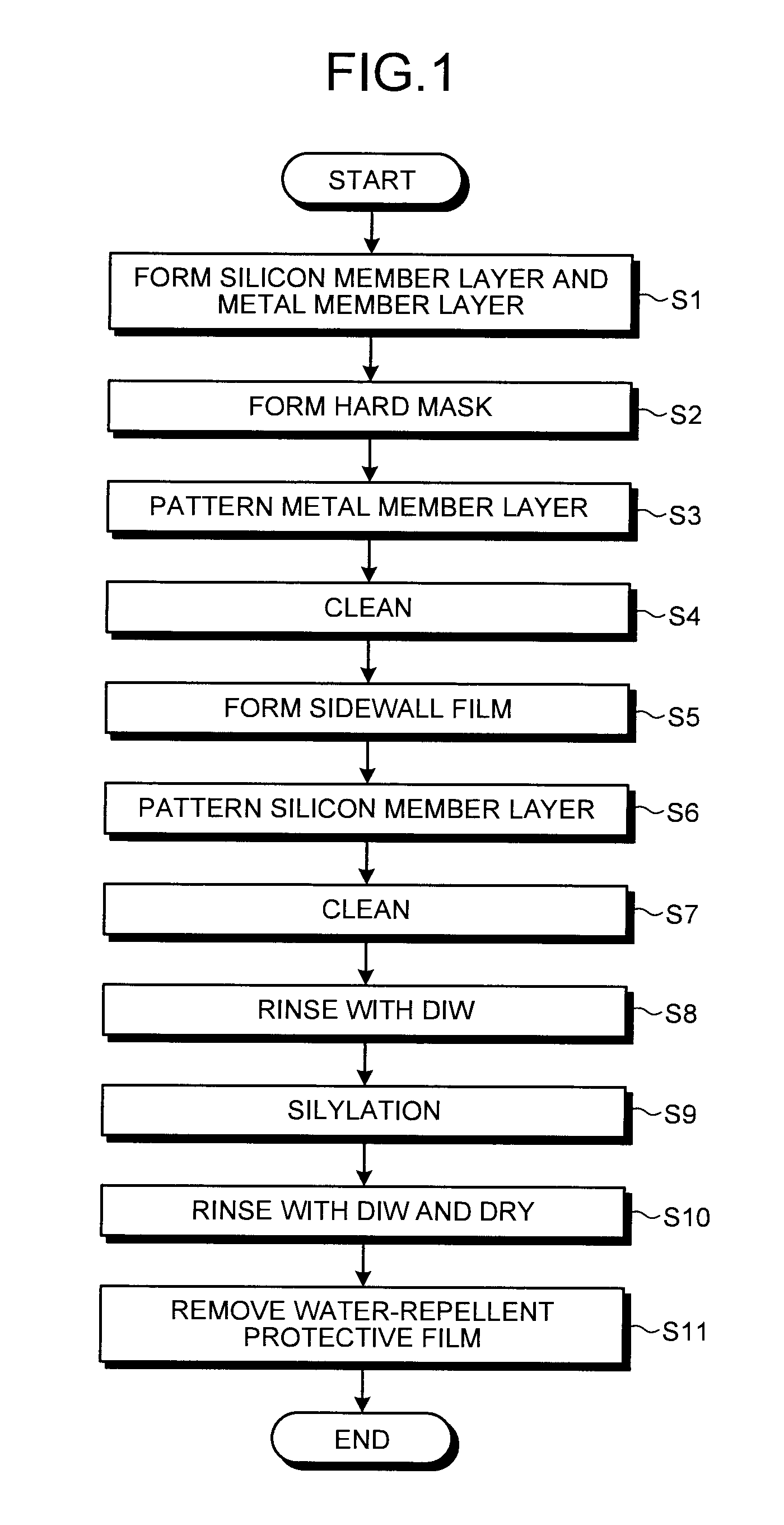
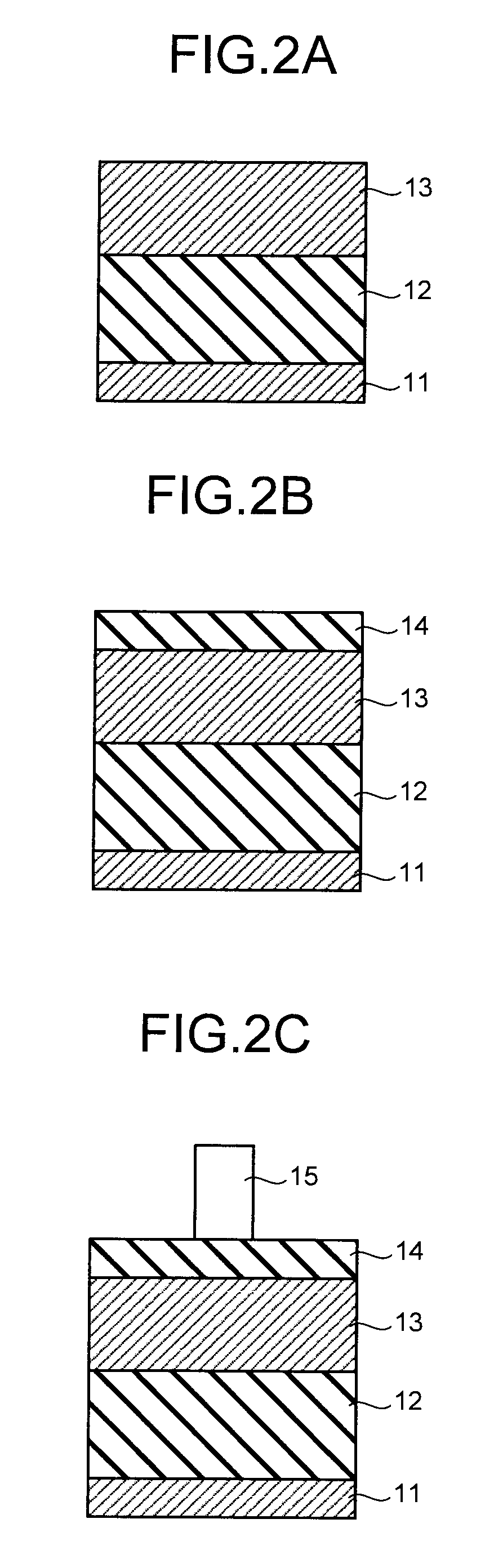
[0018]FIG. 1 is a flowchart for explaining a procedure of a method of manufacturing a semiconductor device according to a first embodiment of the present invention. FIGS. 2A to 2J are schematic sectional views for explaining a process for manufacturing a semiconductor device. In this embodiment, manufacturing of patterns from a structure including a metal member layer 13 in an upper layer and a silicon member layer 12 in a lower layer includes a process for forming a sidewall film 17 and a process for applying silylation treatment. The manufacturing method according to this embodiment is suitable for manufacturing, for example, a resistance random access memory (ReRAM) as a semiconductor device.
[0019]At step S1, as shown in FIG. 2A...
PUM
 Abstract
Description
Claims
Application Information
 - R&D Engineer
- R&D Manager
- IP Professional
- Industry Leading Data Capabilities
- Powerful AI technology
- Patent DNA Extraction
Browse by: Latest US Patents, China's latest patents, Technical Efficacy Thesaurus, Application Domain, Technology Topic, Popular Technical Reports.
© 2024 PatSnap. All rights reserved.Legal|Privacy policy|Modern Slavery Act Transparency Statement|Sitemap|About US| Contact US: help@patsnap.com