
Phase-change memory device and method of manufacturing the phase-change memory device

a memory device and phase-change technology, applied in the direction of bulk negative resistance effect devices, semiconductor devices, electrical devices, etc., can solve the problems of data stored in the memory cell, which is not a data write target, and the memory state of each memory cell is affected,

Inactive Publication Date: 2010-10-28
KK TOSHIBA
View PDF6 Cites 38 Cited by
  • Summary
  • Abstract
  • Description
  • Claims
  • Application Information

AI Technical Summary

Benefits of technology

[0018]wherein each of the memory cells includes a heat source element that is supplied with a current and generates heat and a phase-change element that is changed to an amorphous state or a crystalline state according to a cooling speed after being heated by the heat source element, a resistance value of the phase-change element varying with the change in the state, and

Problems solved by technology

However, when the degree of integration of the memory cells in the same plane is increased, the memory states of each memory cells are affected by heat generated by the heat source elements of adjacent memory cells.
The crystalline states of phase-change elements other than a phase-change element, which is a data write target, are changed by the heat, which causes data stored in the memory cell, which is not a data write target, to be damaged.

Method used


Image

  • Phase-change memory device and method of manufacturing the phase-change memory device
  • Phase-change memory device and method of manufacturing the phase-change memory device
  • Phase-change memory device and method of manufacturing the phase-change memory device

Examples


first embodiment

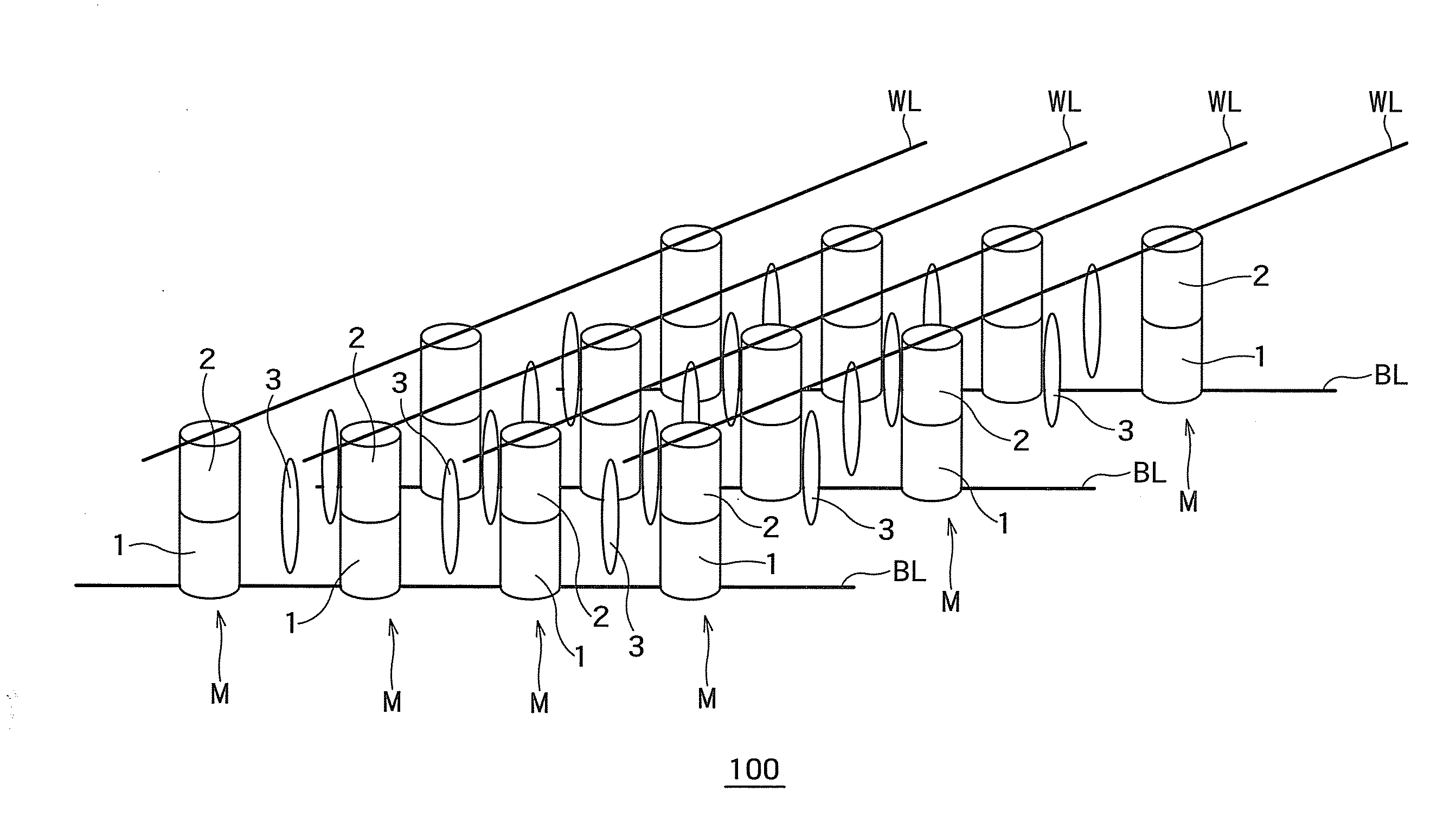
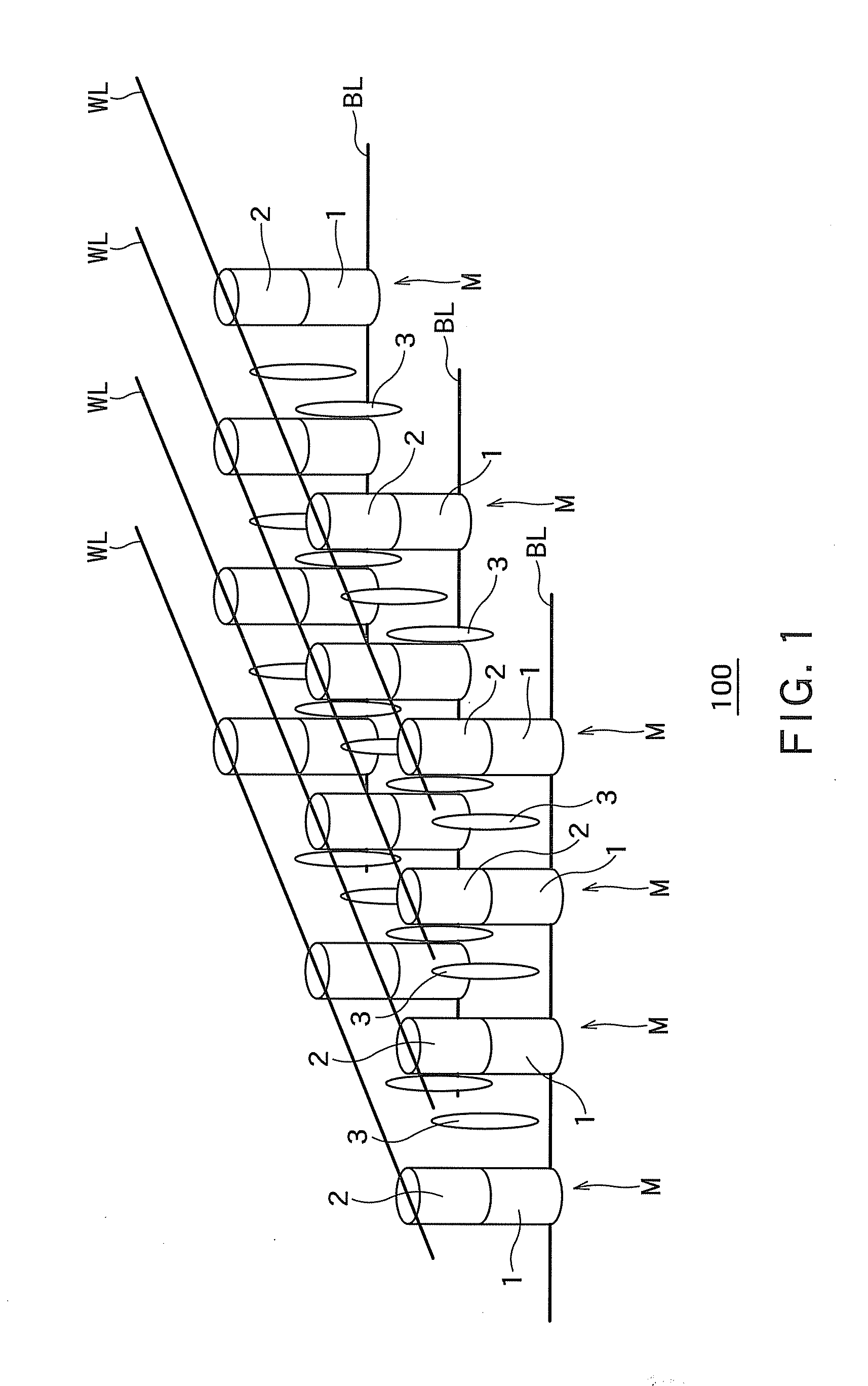
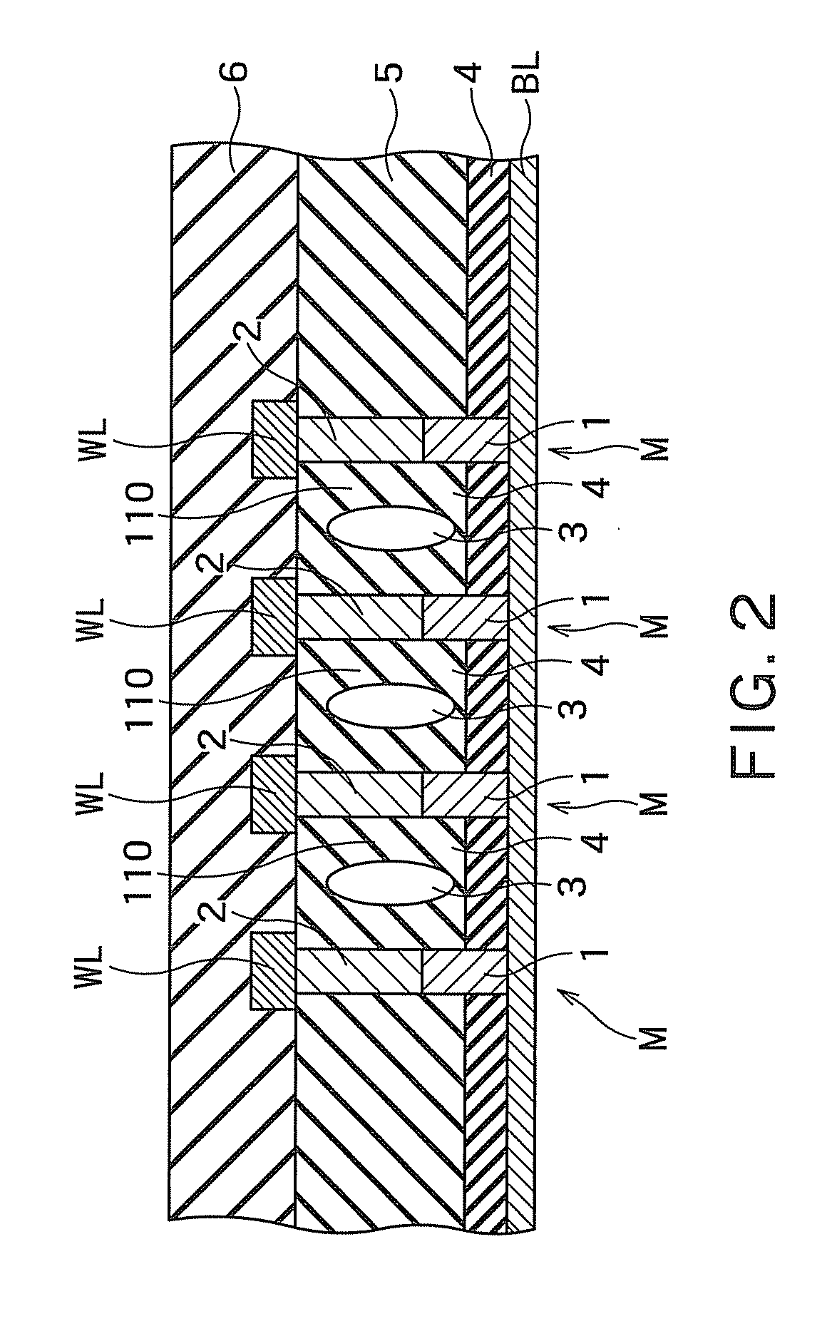
[0067]FIG. 1 is a diagram illustrating a structure in the vicinity of a memory cell region in which a plurality of memory cells M are arranged in a phase-change memory device 100 according to a first embodiment. FIG. 2 is a longitudinal cross-sectional view illustrating a region including the memory cells M arranged along the bit line BL shown in FIG. 1. For convenience, in FIG. 1, the interlayer insulating films shown in FIG. 2 are omitted. In addition, in FIG. 1, the bit lines BL and the word lines WL are briefly shown.

[0068]As shown in FIGS. 1 and 2, the phase-change memory device 100 includes a plurality of bit lines (wiring lines) BL, a plurality of memory cells M, a plurality of word lines (wiring lines) WL, and interlayer insulating films 4, 5, and 6.

[0069]For example, the plurality of bit lines (wiring lines) BL are arranged in parallel to each other on an insulating film (not shown) formed on a semiconductor substrate (not shown).

[0070]The plurality of memory cells M are pr...

second embodiment

[0092]In the first embodiment, an example of the structure for preventing heat generated by the heat source element of a certain memory cell from being transmitted to the phase-change elements of adjacent memory cells has been described.

[0093]In a second embodiment, another example of the structure for preventing heat generated by the heat source element of a certain memory cell being transmitted to the phase-change elements of adjacent memory cells will be described.

[0094]FIG. 6 is a diagram illustrating a structure in the vicinity of a memory cell region in which a plurality of memory cells M are arranged in a phase-change memory device 200 according to the second embodiment. FIG. 7 is a longitudinal cross-sectional view illustrating a region including the memory cells M arranged along the bit lines BL shown in FIG. 6. For convenience, in FIG. 6, the interlayer insulating films shown in FIG. 2 are omitted. In addition, in FIG. 6, bit lines BL and word lines WL are simply presented...

third embodiment

[0117]In the first and second embodiments, an example of the structure for preventing heat generated by the heat source element of a certain memory cell from being transmitted to the phase-change elements of adjacent other memory cells has been described.

[0118]In a third embodiment, still another example of the structure for preventing heat generated by the heat source element of a certain memory cell from being transmitted to the phase-change elements of adjacent other memory cells will be described.

[0119]FIG. 12 is a diagram illustrating a structure in the vicinity of a memory cell region in which a plurality of memory cells M are arranged in a phase-change memory device 300 according to the third embodiment. FIG. 13 is a longitudinal cross-sectional view illustrating a region including the memory cells M arranged along the bit lines BL shown in FIG. 12. For convenience, in FIG. 12, the interlayer insulating films shown in FIG. 13 are omitted. In FIG. 12, bit lines BL and word lin...


PUM


Abstract

A phase-change memory device has a plurality of first wiring lines; a plurality of memory cells that are provided on the plurality of first wiring lines; a plurality of second wiring lines that are provided on the plurality of memory cells, respectively; and an interlayer insulating film that is formed between the plurality of first wiring lines and the plurality of second wiring lines and insulates the plurality of first wiring lines from the plurality of second wiring lines; wherein each of the memory cells includes a heat source element that is supplied with a current and generates heat and a phase-change element that is changed to an amorphous state or a crystalline state according to a cooling speed after being heated by the heat source element, a resistance value of the phase-change element varying with the change in the state, and wherein a void is formed between the two adjacent memory cells in the interlayer insulating film.

Description

CROSS-REFERENCE TO RELATED APPLICATION[0001]This application is based upon and claims the benefit of priority from the prior Japanese Patent Application No. 2009-107334, filed on Apr. 27, 2009, the entire contents of which are incorporated herein by reference.BACKGROUND OF THE INVENTION[0002]1. Field of the Invention[0003]The present invention relates to a phase-change memory device including phase-change elements whose resistance value is changed when its state is changed to an amorphous state or a crystalline state.[0004]2. Background Art[0005]In the conventional art, each of the memory cells of a phase-change memory device, which is a switching structure, includes a heat source element and a phase-change element provided on the heat source element.[0006]The heat source element is supplied with a current and generates heat, and the crystalline state of the phase-change element provided on the heat source element is changed. Specifically, the phase-change element is changed between...

Claims


Application Information

Patent Timeline
Patent Type & Authority Applications(United States)
IPC IPC(8): H01L47/00H01L21/06H10N80/00
CPCH01L27/2463H01L45/06H01L45/1233H01L45/126H01L45/1683H01L45/144H01L45/148H01L45/1675H01L45/1293H10B63/80H10N70/231H10N70/826H10N70/8413H10N70/8616H10N70/8828H10N70/884H10N70/063H10N70/066
Inventor SAWAMURA, KENJI
Owner KK TOSHIBA
Learn More