Semiconductor device

Inactive Publication Date: 2010-10-28
RENESAS ELECTRONICS CORP
View PDF3 Cites 3 Cited by
  • Summary
  • Abstract
  • Description
  • Claims
  • Application Information

AI Technical Summary

Benefits of technology

[0011]As described above, according to the present invention, the coefficient of coupling between two inductors can be increased where electric signals are transferred by inductively coupling the two inductors to each other.

Problems solved by technology

However, it is difficult to reduce the size of each photo coupler due to the existence of the light emitting element and the light receiving element.
Also, where the frequency of electric signals is high, the photo couplers cannot follow the electric signals.
Therefore, it is difficult to increase the diameter of each inductor.
As a result, the coefficient of coupling between two inductors cannot be made larger.

Method used


Image

  • Semiconductor device
  • Semiconductor device
  • Semiconductor device

Examples


first embodiment

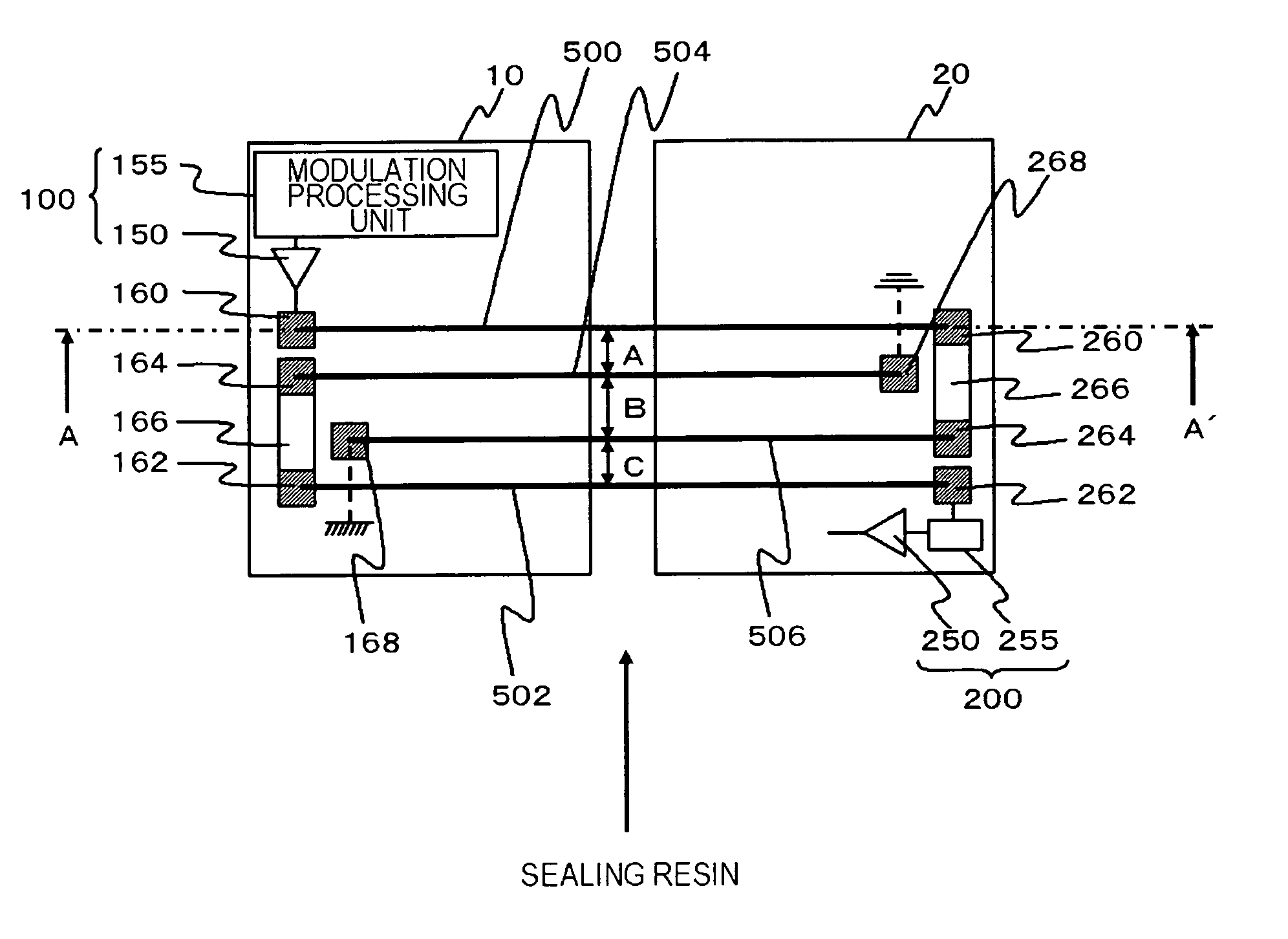
[0022]FIG. 1 is a schematic plan view showing the structure of a semiconductor device according to a first embodiment. This semiconductor device includes a first semiconductor chip 10 as a first region, a second semiconductor chip 20 as a second region, a first inductor, a second inductor, a first bonding wire 500, and a second bonding wire 502.

[0023]The first semiconductor chip 10 includes a transmission circuit 100, a first connecting terminal 160, and a second connecting terminal 162. The second semiconductor chip 20 is placed alongside the first semiconductor chip 10, and has a reference potential isolated from the first semiconductor chip 10. The second semiconductor chip 20 includes a reception circuit 200, a third connecting terminal 260, and a fourth connecting terminal 262. The first inductor is connected to the transmission circuit 100. The second inductor is connected to the reception circuit 200, and is inductively coupled to the first inductor. At least part of the firs...

second embodiment

[0049]FIG. 4 is a schematic plan view showing the structure of a semiconductor device according to a second embodiment. This semiconductor device is the same as the semiconductor device according to the first embodiment, except that each of the first bonding wire 500, the second bonding wire 502, the third bonding wire 506, and the fourth bonding wire 504 of the first embodiment is divided into a plurality of bonding wires.

[0050]More specifically, a first connecting terminal 160, a second connecting terminal 162, a fifth connecting terminal 164, and a sixth connecting terminal 168 are provided on a side of a first semiconductor chip 10, with the side facing a second semiconductor chip 20. A third connecting terminal 260, a fourth connecting terminal 262, a seventh connecting terminal 264, and an eighth connecting terminal 268 are provided on a side of the second semiconductor chip 20, with the side facing the first semiconductor chip 10. The first connecting terminal 160 is not conn...

third embodiment

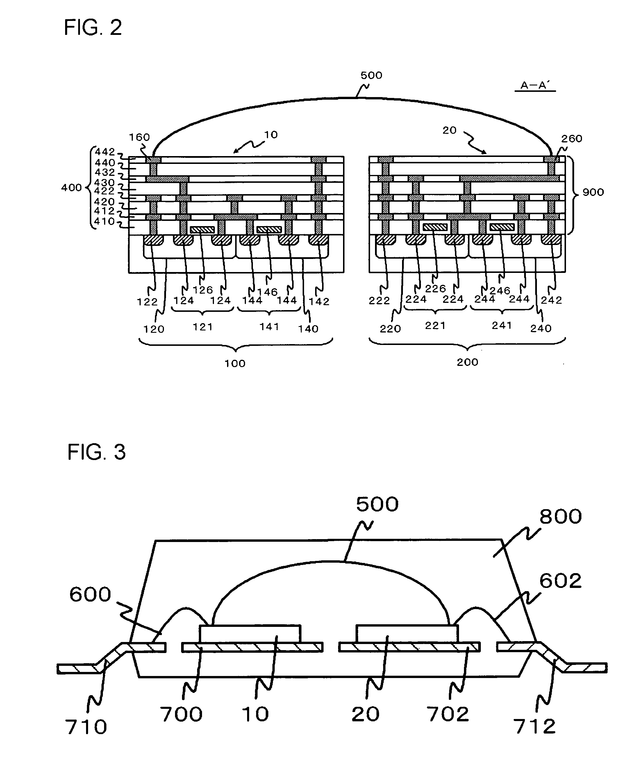
[0067]FIG. 5 is a schematic plan view of a semiconductor device according to a third embodiment. FIG. 6 is a cross-sectional view of the semiconductor device, taken along the line B-B′ of FIG. 5. FIG. 5 is equivalent to FIG. 1 illustrating the first embodiment, and FIG. 6 is equivalent to FIG. 2 illustrating the first embodiment. The semiconductor device according to this embodiment is the same as the semiconductor device according to the first embodiment, except that each of the components formed in the first semiconductor chip 10 and each of the components formed in the second semiconductor chip 20 are formed on a same SOI substrate 101.

[0068]More specifically, each of the components formed in the first semiconductor chip 10 is formed in a first region 12, and each of the components formed in the second semiconductor chip 20 is formed in a second region 22. The first region 12 and the second region 22 have reference potential isolated from each other by an insulating layer 104 tha...


PUM


Abstract

A first inductor is connected to a transmission circuit. A second inductor is connected to a reception circuit, and is inductively coupled to the first inductor. At least part of the first inductor is formed with a first bonding wire. The first bonding wire has two ends connected to a first connecting terminal and a third connecting terminal. At least part of the second inductor is formed with a second bonding wire. The second bonding wire has two ends connected to a second connecting terminal and a fourth connecting terminal.

Description

[0001]This application is based on Japanese patent application No. 2009-101860, the content of which is incorporated herein by reference.BACKGROUND[0002]1. Technical Field[0003]The present invention relates to a semiconductor device that is capable of transferring electric signals between two circuits to which electric signals having different potentials from each other are input.[0004]2. Related Art[0005]To transfer electric signals between two circuits to which electric signals having different potentials from each other are input, photo couplers are often used. Each photo coupler includes a light emitting element such as a light emitting diode and a light receiving element such as a photo transistor. The light emitting element converts an input electric signal into light, and the light receiving element returns the light to an electric signal. In this manner, photo couplers transfer electric signals.[0006]However, it is difficult to reduce the size of each photo coupler due to th...

Claims


Application Information

Patent Timeline
IPC IPC(8): H01L29/86H01F5/00
CPCH01F19/00H01L23/49575H01L23/5227H01L2224/49175H01L2224/48247H01L24/48H01L2224/48137H01L24/06H01L2224/05554H01L2224/48091H01L2924/00014H01L2924/12041H01L2924/181H01L2224/49109H01L24/49H01L2224/45099H01L2924/00H01L2924/00012
Inventor FURUMIYA, MASAYUKINAKASHIBA, YASUTAKA
Owner RENESAS ELECTRONICS CORP
Why Eureka
Try Eureka