
Semiconductor device and method of manufacturing semiconductor device

a semiconductor and semiconductor technology, applied in the direction of semiconductor devices, semiconductor/solid-state device details, electrical devices, etc., can solve problems such as signal delay, and achieve the effect of preventing connection

Active Publication Date: 2010-10-28
RENESAS ELECTRONICS CORP
View PDF7 Cites 24 Cited by
  • Summary
  • Abstract
  • Description
  • Claims
  • Application Information

AI Technical Summary

Benefits of technology

The invention provides a semiconductor device and a method of manufacturing it that prevents connection between an air gap and a via, even if there is positional deviation between the via and an interconnect. This is achieved by using an etching stopper film and a third insulating layer to separate the air gap from the connection hole. The technical effect is to improve the reliability and reliability of semiconductor devices.

Problems solved by technology

When the gap between the interconnects is reduced, the capacitance between the interconnects is increased, which causes a signal delay.

Method used


Image

  • Semiconductor device and method of manufacturing semiconductor device
  • Semiconductor device and method of manufacturing semiconductor device
  • Semiconductor device and method of manufacturing semiconductor device

Examples


first embodiment

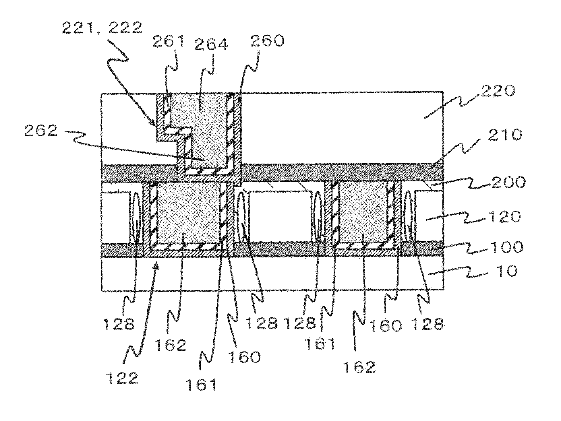
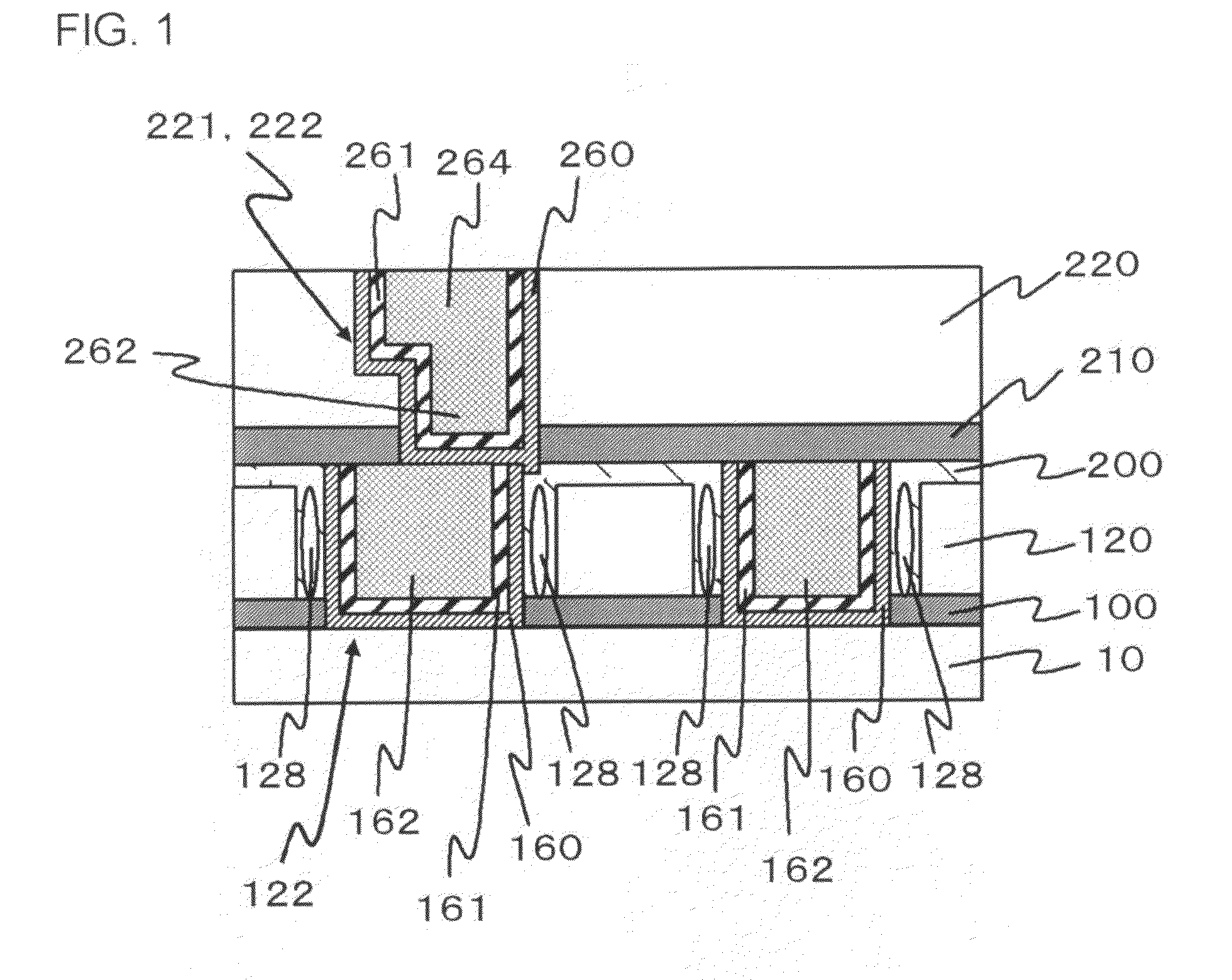
[0031]FIG. 1 is a cross-sectional view illustrating the structure of a semiconductor device according to a first embodiment of the invention. The semiconductor device includes a first insulating layer 120, interconnects 162, air gaps 128, a second insulating layer 200, an etching stopper film 210, a third insulating layer 220, and a via 262. The interconnects 162 are provided in the first insulating layer 120, and the upper surface of the interconnect 162 is higher than the upper surface of the first insulating layer 120. The air gap 128 is disposed between the interconnect 162 and the first insulating layer 120. The second insulating layer 200 is formed at least on the first insulating layer 120 and the air gaps 128. In the example shown in FIG. 1, the second insulating layer 200 does not cover the interconnect 162. The etching stopper film 210 is formed at least on the second insulating layer 200. In the example shown in FIG. 1, the etching stopper film 210 is formed on the second...

second embodiment

[0058]FIG. 7 is a cross-sectional view illustrating the structure of a semiconductor device according to a second embodiment of the invention. The semiconductor device has the same structure as that according to the first embodiment except for the following points. First, the underlying insulating film 10 is an insulating film in which a via connected to the interconnect 162 is formed. Therefore, the etching stopper film 100 according to the first embodiment is not formed between the underlying insulating film 10 and the first insulating layer 120.

[0059]The third insulating layer 220 includes an insulating interlayer 224 and an interconnect layer insulating layer 226. The via 262 is provided in the insulating interlayer 224, and the interconnect 264 is provided in the interconnect layer insulating layer 226. An air gap 302 is formed between the interconnect 264 and the interconnect layer insulating layer 226, and an insulating layer 300 and an etching stopper film 310 are formed on ...

third embodiment

[0061]FIGS. 8A to 10 are cross-sectional views illustrating a method of manufacturing a semiconductor device according to a third embodiment of the invention. As shown in FIG. 10, the semiconductor device manufactured by the method has the same structure as the semiconductor device according to the first embodiment except that a metal cap film 164 is provided on the interconnect 162. The metal cap film 164 is, for example, a CoWP film. Alternatively, the metal cap film 164 may be a CoWB film or a film plated with a Ni-based material.

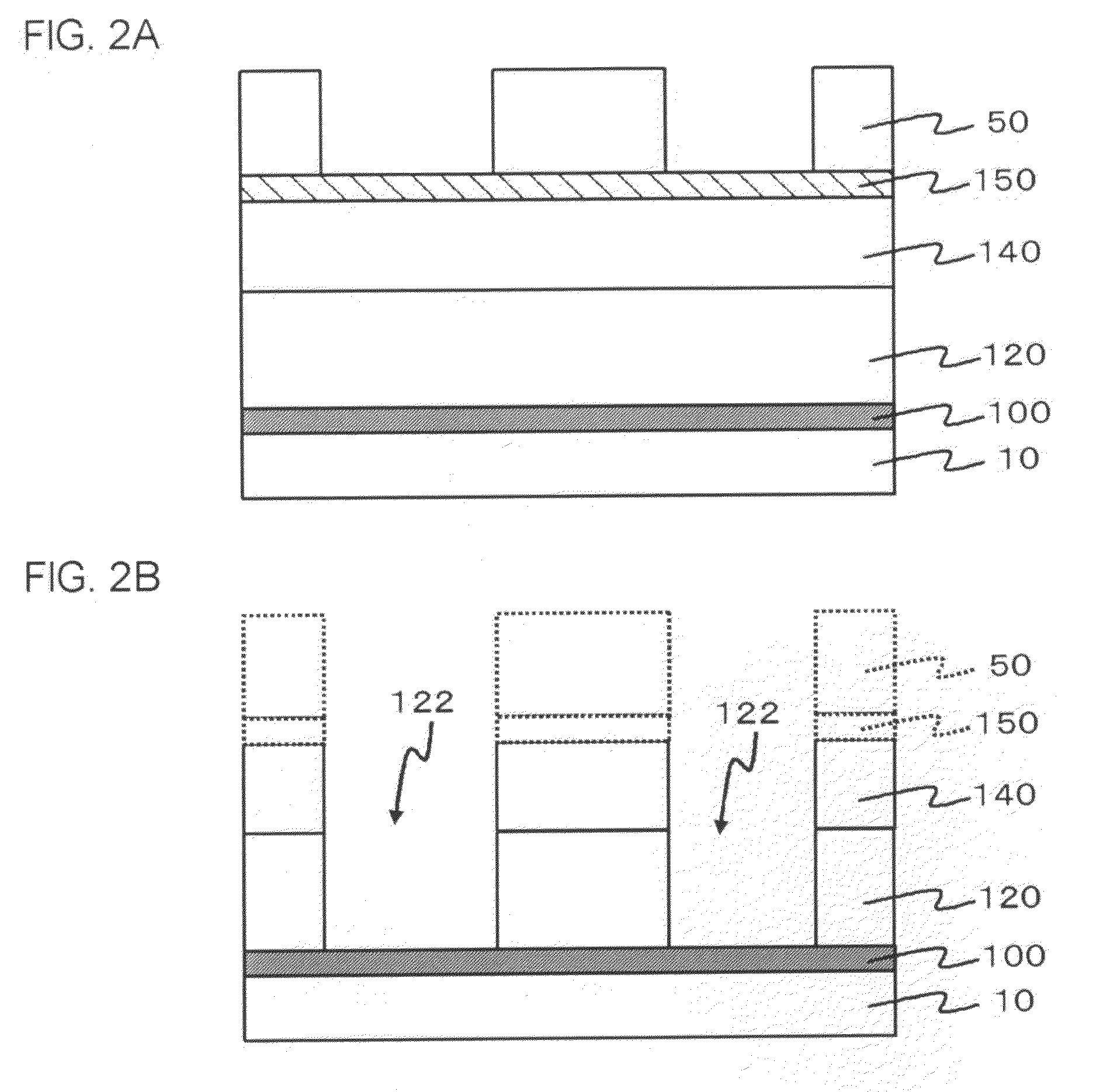
[0062]First, as shown in FIG. 8A, the etching stopper film 100, the first insulating layer 120, the grooves 122, the first damaged layer 124, the diffusion barrier metal film 160, the seed film 161, and the interconnects 162 are formed on the underlying insulating film 10. A process of forming the components is the same as that in the first embodiment.

[0063]Then, as shown in FIG. 8B, the metal cap film 164 is selectively formed on the interconnect 162 by...


PUM


Abstract

An interconnect is provided in a first insulating layer and the upper surface of the interconnect is higher than the upper surface of the first insulating layer. An air gap is disposed between the interconnect and the first insulating layer. A second insulating layer is formed at least over the first insulating layer and the air gap. The second insulating layer does not cover the interconnect. An etching stopper film is formed at least over the second insulating layer. The etching stopper film is formed over the second insulating layer and the interconnect. A third insulating layer is formed over the etching stopper film. A via is provided in the third insulating layer so as to be connected to the interconnect.

Description

[0001]The application is based on Japanese patent application No. 2009-106389, the content of which is incorporated hereinto by reference.BACKGROUND[0002]1. Technical Field[0003]The present invention relates to a semiconductor device in which an air gap is provided between an interconnect and an insulating film having the interconnect provided therein and a method of manufacturing a semiconductor device.[0004]2. Related Art[0005]With the reduction in the size of semiconductor devices, the gap between interconnects has been reduced. When the gap between the interconnects is reduced, the capacitance between the interconnects is increased, which causes a signal delay. As an example of a technique for reducing the capacitance between the interconnects, an air gap is provided between the interconnect and an insulating film having the interconnect provided therein.[0006]U.S. Published patent application NO. 2008 / 0076258 discloses a structure in which, when a groove in which an interconnec...

Claims


Application Information

Patent Timeline
Patent Type & Authority Applications(United States)
IPC IPC(8): H01L23/48H01L21/768
CPCH01L21/76807H01L21/7682H01L21/76826H01L21/76829H01L21/76835H01L2924/0002H01L23/5222H01L23/53295H01L21/76849H01L2924/00H01L2221/1063
Inventor USAMI, TATSUYA
Owner RENESAS ELECTRONICS CORP
Learn More