Waveguide Coupling Probe and Methods for Manufacturing Same

a coupling probe and waveguide technology, applied in the field of integrated optical circuits, can solve the problems of inability to integrate optical circuits, inconvenient manufacturing, time-consuming and permanent dicing, etc., and achieve the effect of avoiding the provision of coupling structures on the substra

Inactive Publication Date: 2010-11-04
INTERUNIVERSITAIR MICRO ELECTRONICS CENT (IMEC VZW) +1
View PDF22 Cites 26 Cited by
  • Summary
  • Abstract
  • Description
  • Claims
  • Application Information

AI Technical Summary

Benefits of technology

[0008]It is an aim of the present invention to provide a waveguide coupling probe for sending light into an optical waveguide on a substrate, e.g. a substrate comprising an integrated optical circuit, and/o

Problems solved by technology

However, each of these methods has distinct disadvantages when the coupling scheme is applied for wafer-scale testing of high-index-contrast as well as low-index-contrast optical components and circuits.
However, dicing is time consuming and permanent.
The effort is useless if, after testing, it turns out that the integrated optical circuit is not working.
Testing of individual components in the optical circuit is not possible with this method.
Testing of individual components is not possible using this method.
This method becomes extremely challenging for testing high-index

Method used


Image

  • Waveguide Coupling Probe and Methods for Manufacturing Same
  • Waveguide Coupling Probe and Methods for Manufacturing Same
  • Waveguide Coupling Probe and Methods for Manufacturing Same

Examples


Embodiment Construction

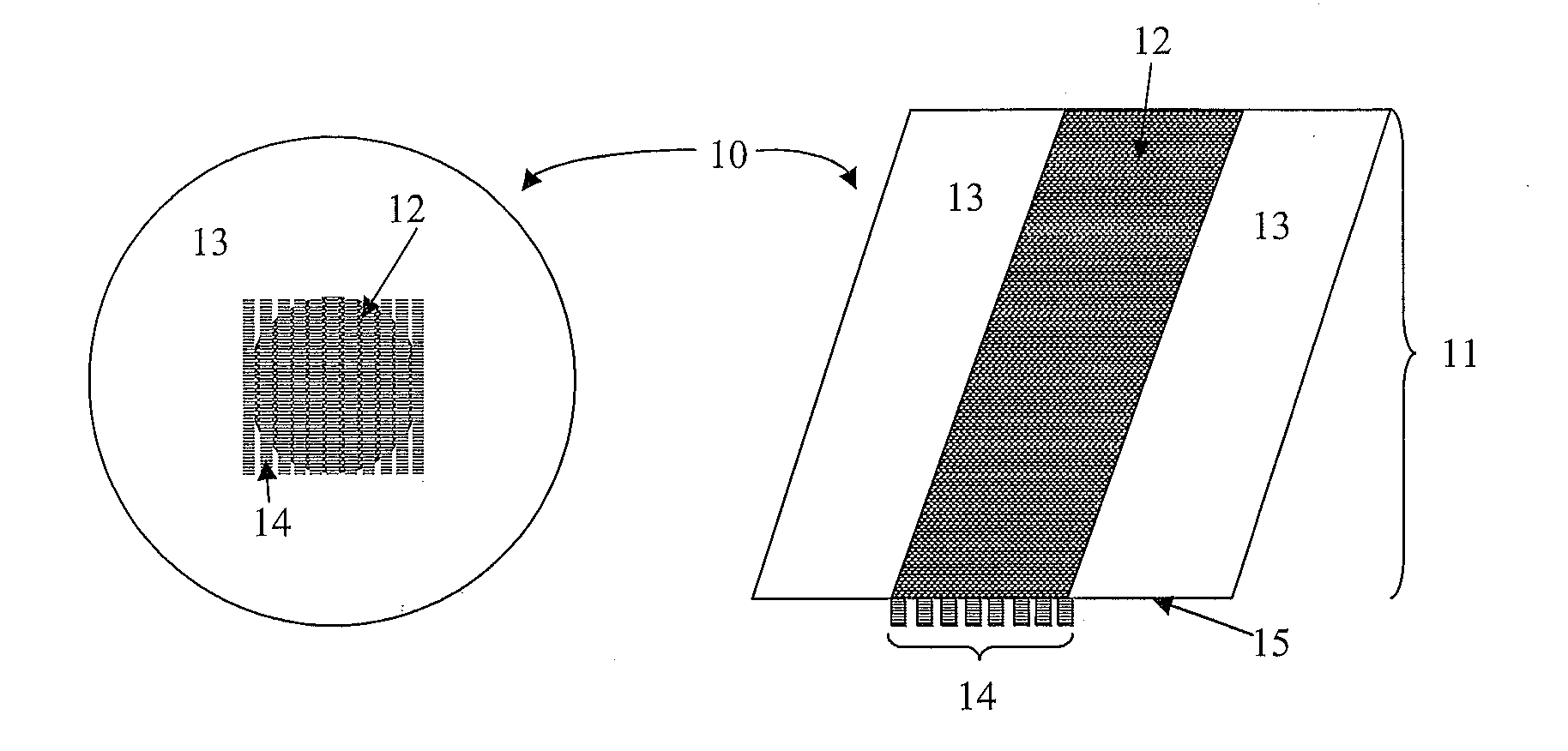
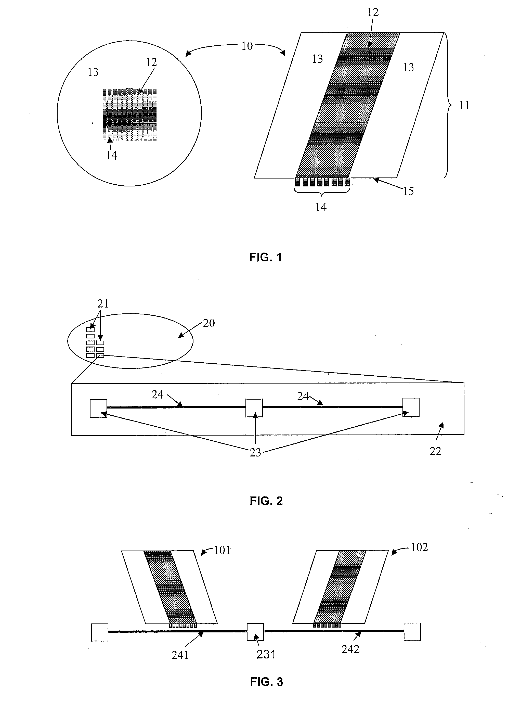
[0054]In the following detailed description, numerous specific details are set forth in order to provide a thorough understanding of the invention and how it may be practiced in particular embodiments. However it will be understood that the present invention may be practiced without these specific details. In other instances, well-known methods, procedures and techniques have not been described in detail, so as not to obscure the present invention. While the present invention will be described with respect to particular embodiments and with reference to certain drawings, the reference is not limited hereto. The drawings included and described herein are schematic and are not limiting the scope of the invention. It is also noted that in the drawings, the size of some elements may be exaggerated and, therefore, not drawn to scale for illustrative purposes.

[0055]Furthermore, the terms first, second and the like in the description and in the claims, are used for distinguishing between s...


PUM


Abstract

A waveguide coupling probe (10) for sending light into an optical waveguide on a substrate or for receiving light from an optical waveguide on a substrate is provided, the waveguide coupling probe comprising an optical element (11) for guiding the light in a propagation direction, the optical element (11) having a facet (15) where the light enters or exits the optical element (11) and means for coupling the light between the optical element (11) and the waveguide. A waveguide coupling probe (10) according to the present invention is characterized in that the light coupling means are formed on the facet (15) and comprise a diffraction structure (14). In a preferred embodiment the optical element (11) may be an optical fiber and the diffraction structure may be a strong diffraction structure, e.g. a metal grating structure. When bringing the waveguide coupling probe (10) in the vicinity of a waveguide on a substrate, the light that is guided by the waveguide may be diffracted into the optical element (11). Alternatively, light from the optical element (11) may be coupled into the waveguide. When using the waveguide coupling probe (10) for coupling light between the optical element (11) and a waveguide, the waveguide coupling probe may be positioned out of the plane of the waveguide. Furthermore a method is provided for forming an optical structure, e.g. a metal grating structure, on a facet (15) of an optical element (11).

Description

FIELD OF THE INVENTION[0001]The present invention is related to integrated optical circuits. More specifically, it is related to a waveguide coupling probe for sending light into and / or receiving light from an optical waveguide on an integrated optical circuit and to methods for manufacturing such a waveguide coupling probe.[0002]The waveguide coupling probe may for example be used for testing the operation and performance of highly integrated optical components on a wafer scale or it may for example be used in a packaging process for integrated optical circuits. The present invention is furthermore related to a method for sending light into an optical waveguide and / or for receiving light from an optical waveguide.BACKGROUND OF THE INVENTION[0003]There exist numerous methods to send light (e.g., light from an optical fiber) into optical waveguides and / or to receive light from optical waveguides (e.g., high-index-contrast waveguides such as Silicon-on-Insulator based waveguides or lo...

Claims


Application Information

Patent Timeline
IPC IPC(8): G02B6/34B29D11/00
CPCG01M11/35G02B6/34G02B6/30
Inventor SCHEERLINCK, STIJNVAN THOURHOUT, DRIESBAETS, ROELAND
Owner INTERUNIVERSITAIR MICRO ELECTRONICS CENT (IMEC VZW)
Why Eureka
Try Eureka