Pixel circuit, display apparatus, and driving method for pixel circuit

a technology of pixel circuit and display apparatus, which is applied in the direction of electric digital data processing, instruments, computing, etc., can solve the problems of emitted light luminance degrading with time, not only the driving voltage but also the light emission efficiency drop, etc., to reduce the current arising from the dispersion of the operating point of the light detection element, and reduce the influence of mobility

Inactive Publication Date: 2010-11-18
JOLED INC
View PDF8 Cites 9 Cited by
  • Summary
  • Abstract
  • Description
  • Claims
  • Application Information

AI Technical Summary

Benefits of technology

[0023]Here, if the driving transistor Td is formed from an n-channel TFT, then it becomes possible to use a related art amorphous silicon (a-Si) process in TFT fabrication. This makes it possible to reduce the cost of a TFT substrate and obtain a large screen.
[0049]In this pixel circuit, if the light emitting time of the organic EL element 1 becomes long, then the I-V characteristic of the organic EL element 1 varies and also the efficiency varies. Therefore, also the potential at a point B shown in FIG. 16C varies. However, the gate-source voltage Vgs of the driving transistor Td is kept at a fixed value by the holding capacitor Cs and besides the light detection element D1 varies the gate-source voltage Vgs of the driving transistor Td depending upon the emitted light luminance of the organic EL element 1. Therefore, it is possible to establish a state wherein the emitted light luminance of the organic EL element 1 does not vary. Therefore, even if the I-V characteristic or the light emission efficiency of the organic EL element 1 degrades, the luminance of the organic EL element 1 does not vary.
[0052]Therefore, it is desirable to provide a pixel circuit, a display apparatus and a driving method for the pixel circuit wherein a dispersion in adjustment operation by a light detection element can be eliminated so that a display image of high quality can be obtained.
[0059]In the pixel circuit and the driving method, the voltage across the light detection element can be controlled appropriately. Consequently, the influence of the voltage applied to the light detection element by the threshold value correction operation can be eliminated and also the influence of the mobility can be reduced.
[0060]With the pixel circuit, display apparatus and driving method for a pixel circuit, the influence of the threshold voltage of the driving transistor on the voltage to be applied to the light detection element for detecting emitted light from the light emitting element such as an organic EL element can be eliminated and also the influence of the mobility can be reduced. Therefore, it is possible to substantially fix the voltage to be applied to the light detection element, and the dispersion in current arising from a dispersion in operating point of the light detection element can be reduced. Consequently, an emitted light adjustment operation free from a dispersion for each pixel is implemented, and correction against a screen burn can be carried out with a higher degree of accuracy and a uniform image of high picture quality can be achieved.

Problems solved by technology

However, the organic EL element 1 suffers from a drop not only of the driving voltage but also of the light emission efficiency as time passes.
In particular, even if the same current flows, the emitted light luminance degrades together with passage of time.

Method used


Image

  • Pixel circuit, display apparatus, and driving method for pixel circuit
  • Pixel circuit, display apparatus, and driving method for pixel circuit
  • Pixel circuit, display apparatus, and driving method for pixel circuit

Examples


second embodiment

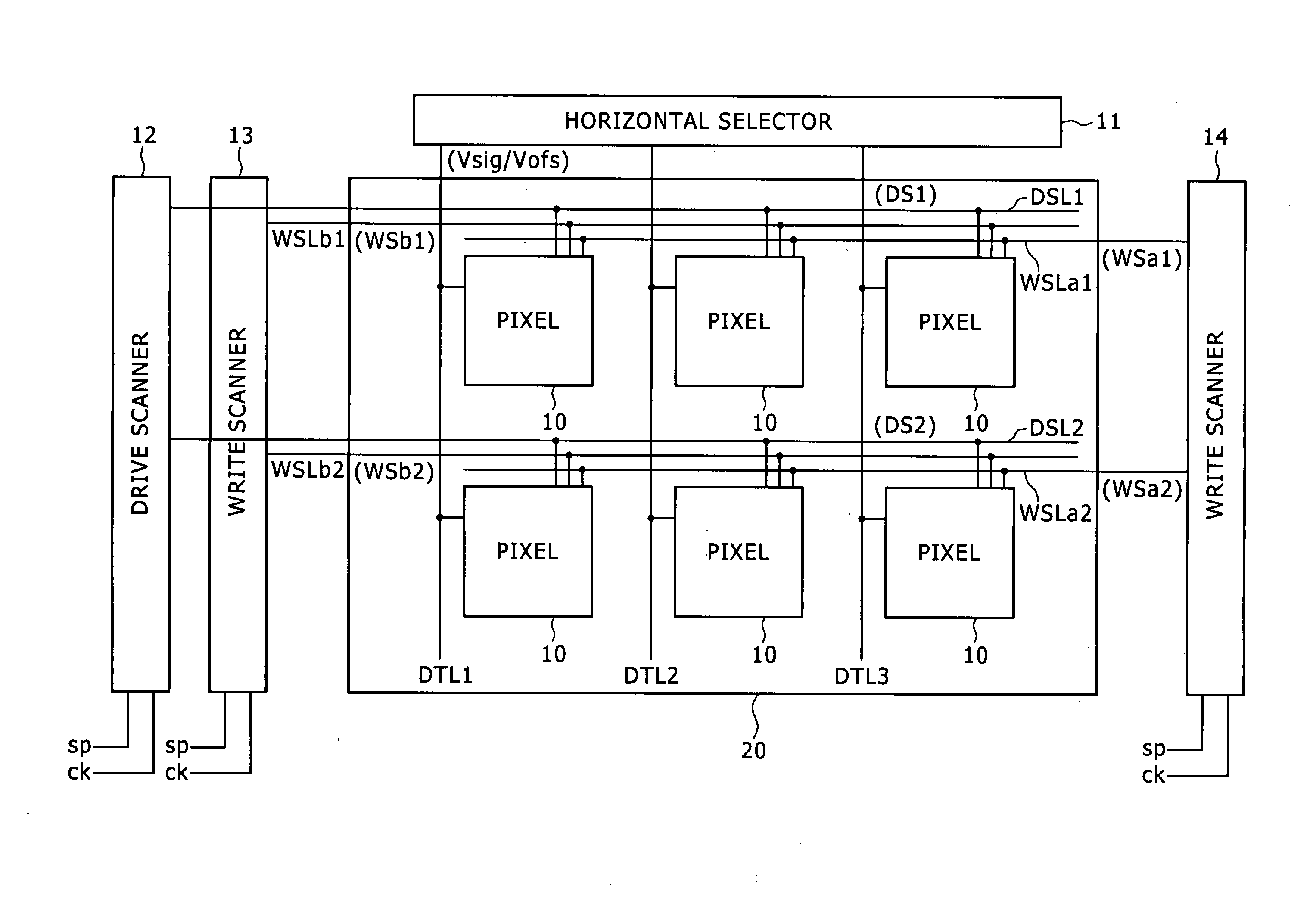
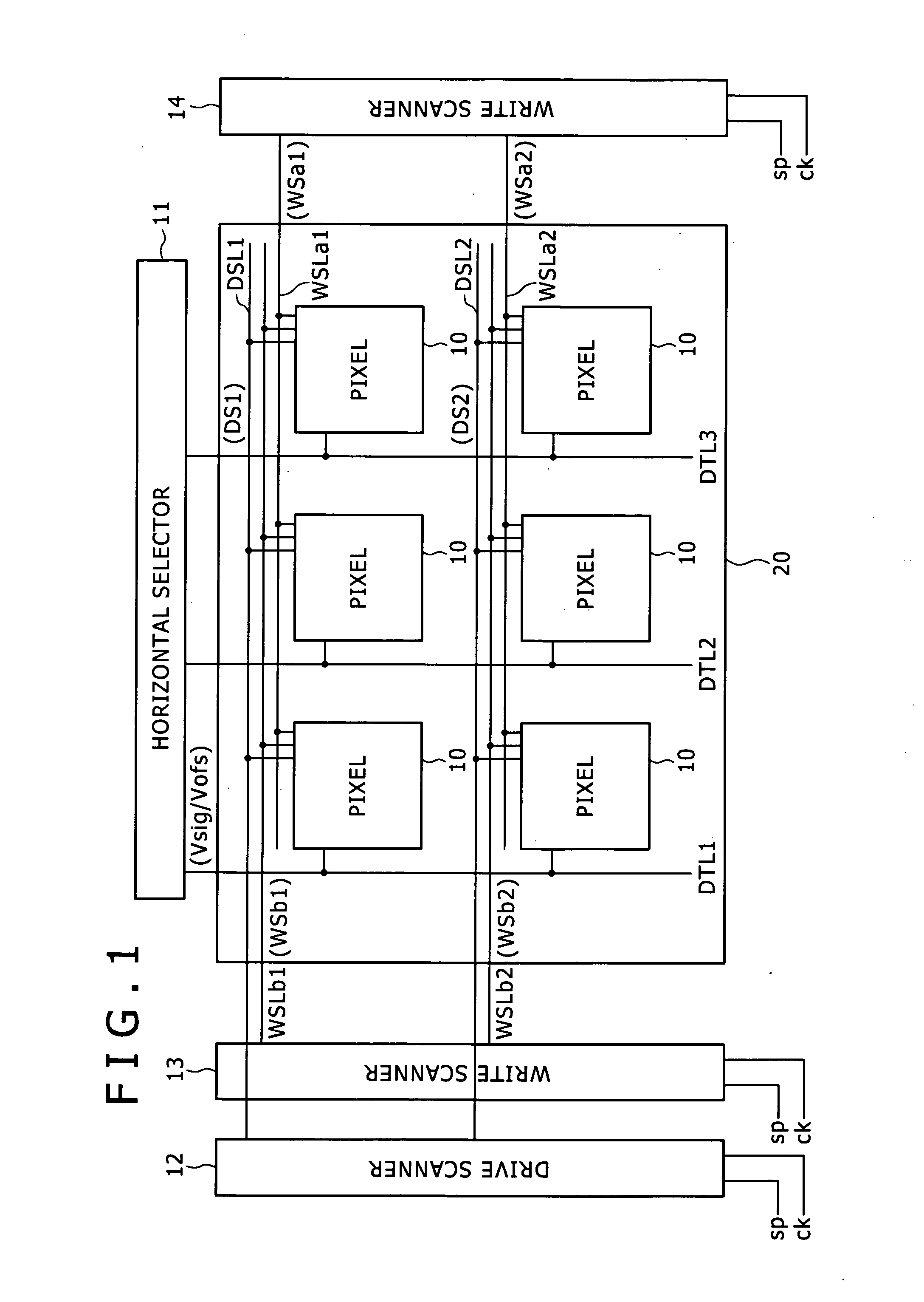
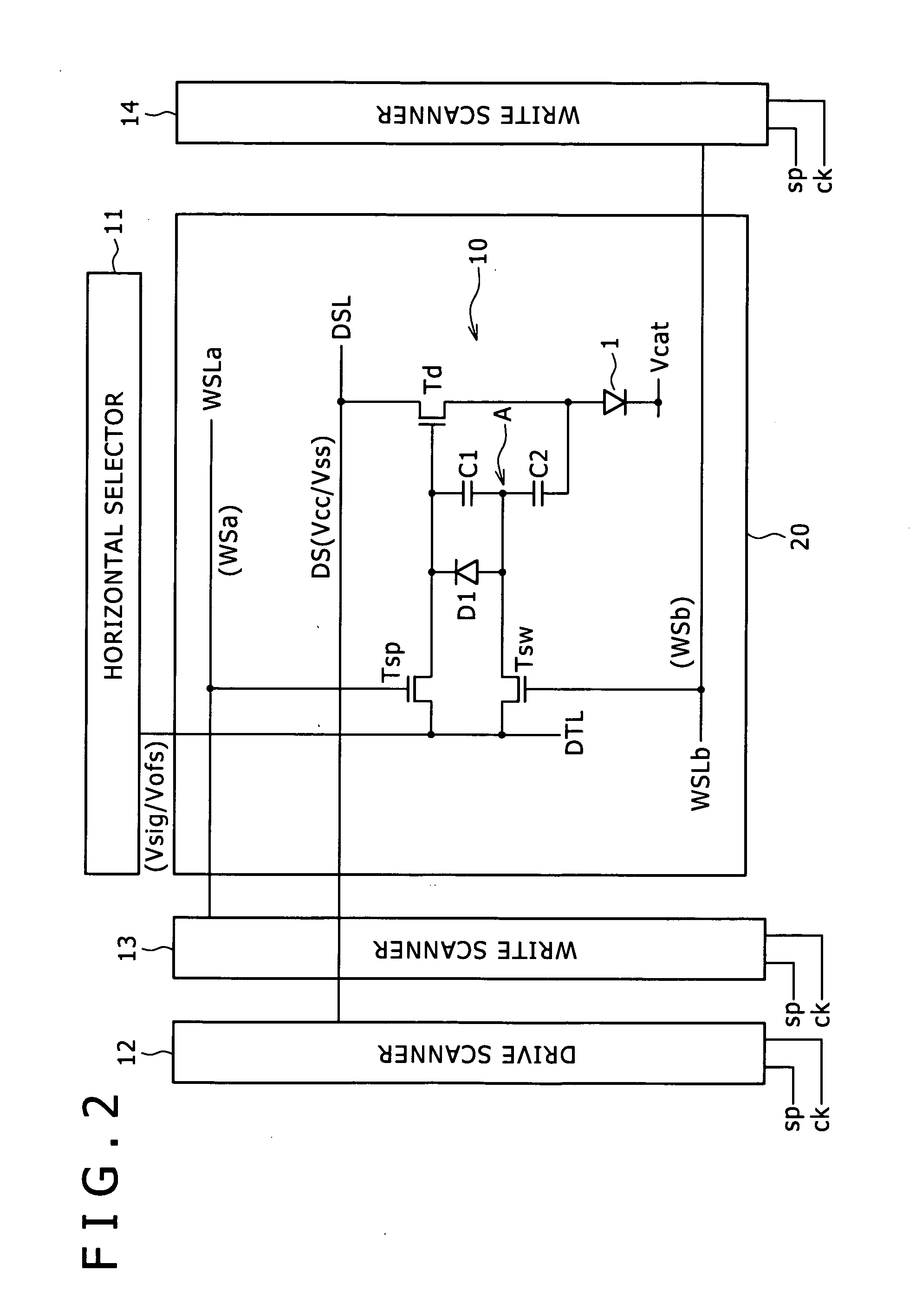
[0148]An example of a configuration of a second pixel circuit 10 according to the present invention is shown in FIG. 6.

[0149]The configuration of the pixel circuit 10 shown in FIG. 6 is similar to that of the first pixel circuit configuration except that the source and the drain of the switching transistor Tsw are connected to the opposite ends of the light detection element D1.

[0150]In other words, the switching transistor Tsw is connected to the node between the two capacitors C1 and C2 and the gate of the driving transistor Td.

[0151]The configuration of the other part and the circuit operation of the pixel circuit are similar to those described hereinabove with reference to FIGS. 2 to 5C.

[0152]In this instance, since the switching transistor Tsw is not connected to the signal line DTL, the parasitic capacitance of the signal line DTL can be reduced. This is advantageous in increase of operation speed, increase of the definition and increase of the size of the screen of the displa...

third embodiment

[0153]A circuit configuration of a third pixel circuit according to the present invention is described with reference to FIGS. 7 and 8.

[0154]The pixel circuit 10 shown in FIG. 7 has a similar configuration to that described hereinabove with reference to FIG. 2 but is different in that a detection period controlling transistor Tks is inserted between the gate of the driving transistor Td and the light detection element D1.

[0155]In particular, the light detection element D1 and the detection period controlling transistor Tks are connected in series between the gate of the driving transistor Td and the node between the capacitors C1 and C2.

[0156]Further, as scanners for driving the pixel circuits, a detection period control scanner 15 is provided in addition to the drive scanner 12 and write scanners 13 and 14.

[0157]Meanwhile, detection period controlling lines PPL are provided individual lines on the pixel array 20 such that they extend in the direction of a row, and the detection per...


PUM


Abstract

A pixel circuit includes: a light emitting element; a driving transistor for applying current to the light emitting element in response to a signal value applied between a gate and a source thereof when a driving voltage is applied between a drain and the source thereof; first and second capacitors connected in series between the gate and the source of the driving transistor; a sampling transistor connected between the gate of the driving transistor and a predetermined signal line; a switching transistor connected to supply a potential of the signal line to a node between the first and second capacitors; and a light detection element connected between the gate of the driving transistor and the node between the first and second capacitors for supplying current of a current amount in accordance with an emitted light amount of the light emitting element.

Description

BACKGROUND OF THE INVENTION[0001]1. Field of the Invention[0002]This invention relates to a pixel circuit formed using, for example, an organic electroluminescence element, that is, an organic EL element, a display apparatus having a pixel array wherein such pixel circuits are disposed in a matrix, and a driving method for the pixel circuit.[0003]Japanese Patent Laid-Open Nos. 2003-255856 and 2003-271095 are known as related art documents to the inventor.[0004]2. Description of the Related Art[0005]In a display apparatus of the active matrix type wherein an organic electroluminescence (EL) light emitting element is used in a pixel, current to flow through a light emitting element in each pixel circuit is controlled by an active element, usually a thin film transistor (TFT), provided in the pixel circuit. In particular, since an organic EL element is a current light emitting element, a gradation of emitted light is obtained by controlling the amount of current to flow through the EL ...

Claims


Application Information

Patent Timeline
Patent Type & Authority Applications(United States)
IPC IPC(8): G09G5/00
CPCG09G3/3233G09G2300/0417G09G2300/0819G09G2360/148G09G2300/0852G09G2320/046G09G2300/0842
Inventor YAMAMOTO, TETSUROUCHINO, KATSUHIDE
Owner JOLED INC
Why Eureka
Try Eureka