
Resistance measuring device, display panel, and measuring method of bonding resistance

a technology of resistance and measuring device, applied in the direction of resistance/reactance/impedence, measurement device, instrument, etc., can solve the problems of affecting the operation efficiency of the display panel, the inability to effectively measure the bonding performance and the inability to use simple methods or equipment to effectively measure the bonding resistance or bonding resistance of acf. the effect of simple steps

Inactive Publication Date: 2010-11-25
CHUNGHWA PICTURE TUBES LTD
View PDF2 Cites 33 Cited by
  • Summary
  • Abstract
  • Description
  • Claims
  • Application Information

AI Technical Summary

Benefits of technology

[0005]Therefore, the primary objective of the present invention is to provide a resistance measuring device and a measuring method thereof applied to display panels, which only require transistors and conductive lines disposed between the bonding pads of the display panel and the bumps of IC chips to directly measure the bonding resistance between the bonding pads and IC chips easily through simple steps.

Problems solved by technology

However, in the manufacturing process of flat display panels, it is uneasy to use simple methods or equipment to effectively measure the bonding performance or bonding resistance of ACF.
However, the extra testing bonding pads may affect the operation efficiency of the display panel and the bonding resistance of ACF may not be measured directly yet.

Method used


Image

  • Resistance measuring device, display panel, and measuring method of bonding resistance
  • Resistance measuring device, display panel, and measuring method of bonding resistance
  • Resistance measuring device, display panel, and measuring method of bonding resistance

Examples


Embodiment Construction

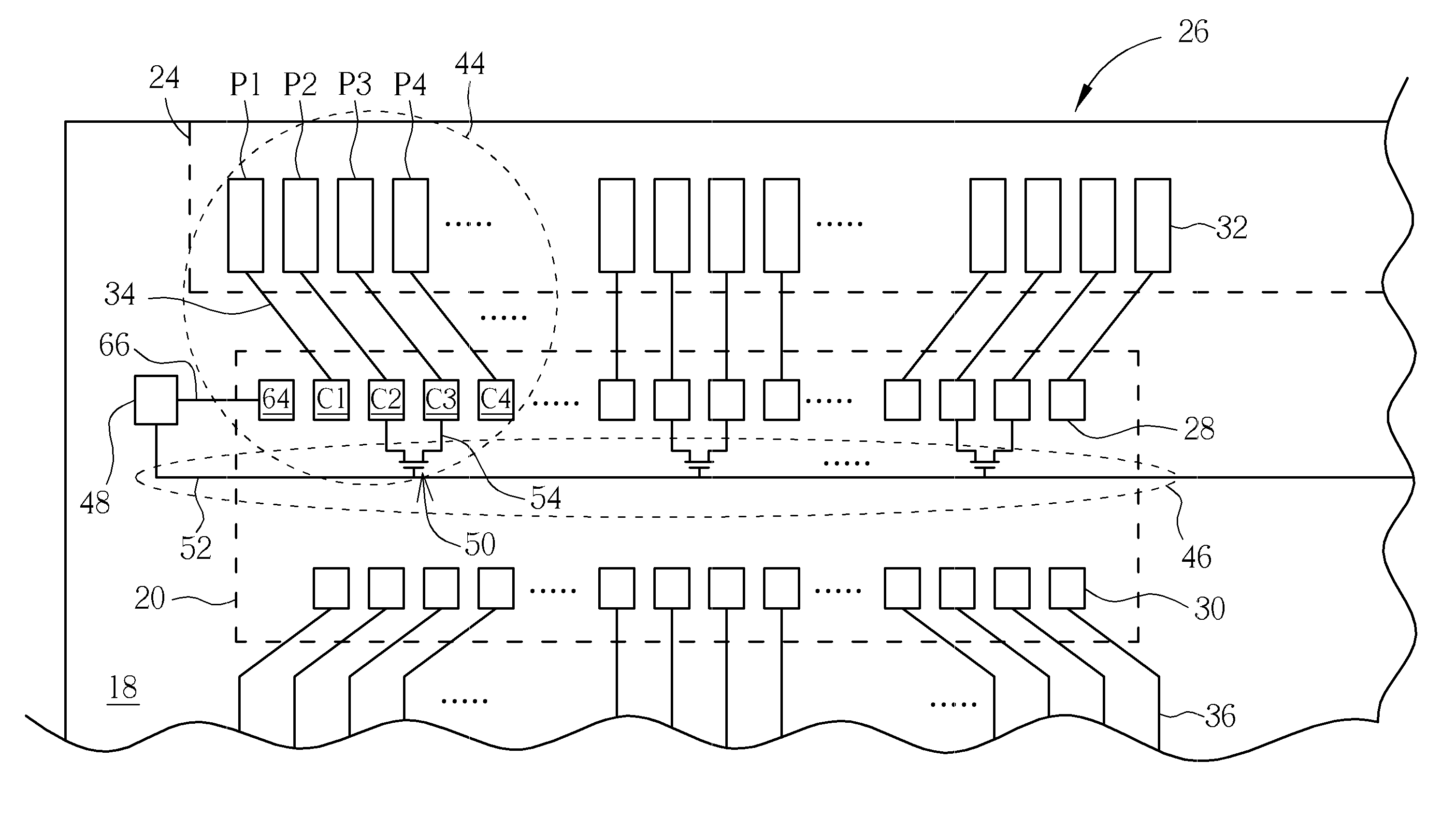
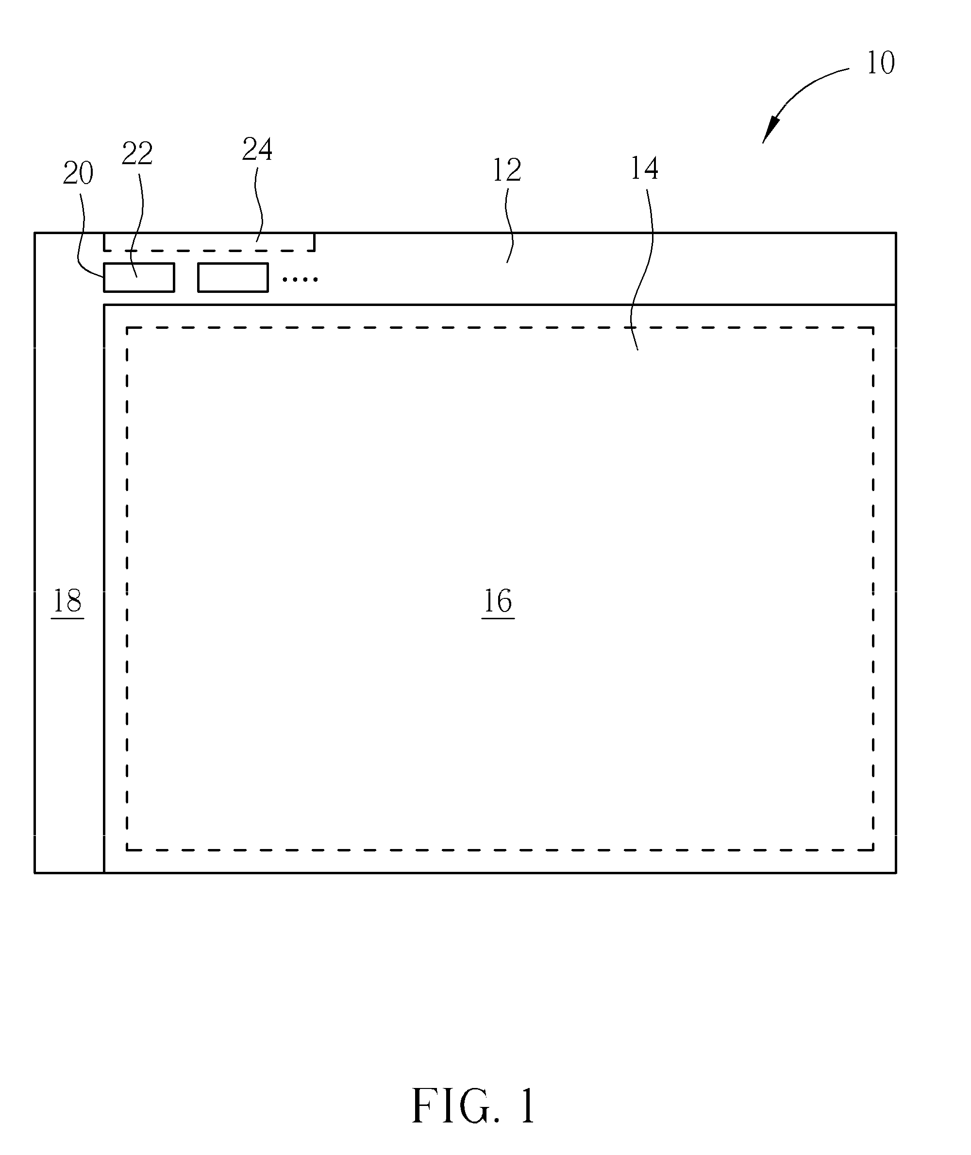
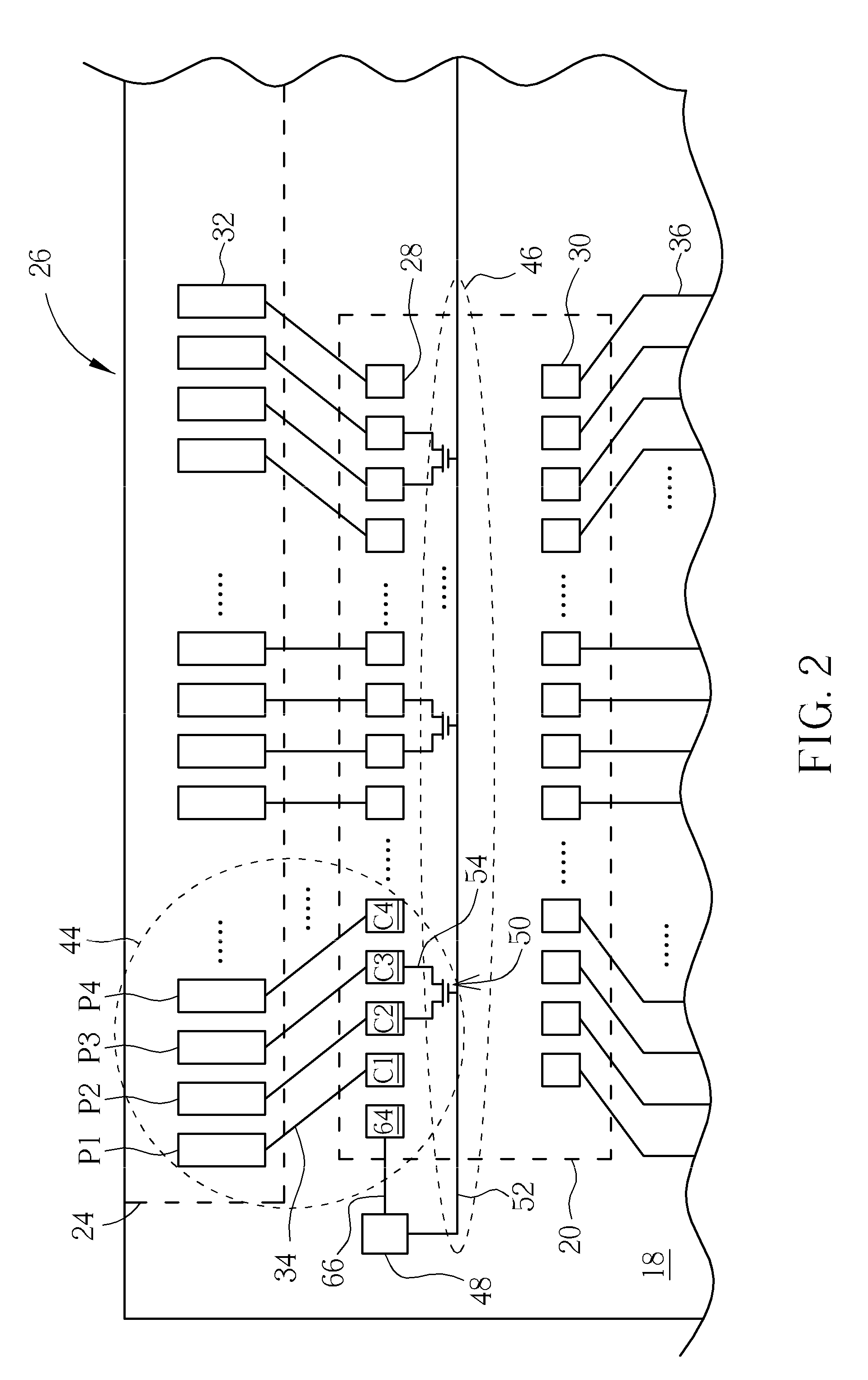
[0056]Referring to FIG. 1, FIG. 1 is a schematic diagram of the top view of a flat display panel of the present invention. The flat display panel 10 of the present invention is a chip-on-glass (COG) display panel, and may be, but not limited to, an LCD panel, a plasma display panel, or an electroluminescent display panel. The flat display panel 10 comprises a lower substrate 12 and an upper substrate 14 that covers a portion of the lower substrate 12. The overlapping area of the lower and upper substrates 12 and 14 is defined as the display region 16 of the flat display panel 10. The portion of the lower substrate 12 which is not covered by the upper substrate 14 is defined as a periphery circuit region 18. The periphery circuit region 18 comprises at least a chip bonding area 20 and a flexible printed circuit (FPC) bonding area 24. An IC chip 22 is disposed in the chip bonding area 20, and at least a FPC (not shown) may be disposed in the FPC bonding area 24 for delivering external...


PUM


Abstract

The resistance measuring device of the present invention includes switch transistors and switch conductive lines disposed between the bonding pads on a first substrate and between the bumps on a second substrate, such that the bonding pads and the bumps are conducted when the transistors are turned on, and the bonding resistance between at least one of the bonding pads and its corresponding bump can be directly measured.

Description

BACKGROUND OF THE INVENTION[0001]1. Field of the Invention[0002]This invention is related to a resistance measuring device and a measuring method of bonding resistance, and more particularly, to a resistance measuring device and a measuring method of bonding resistance of the surface of a display panel.[0003]2. Description of the Prior Art[0004]Comparing to traditional displays, flat display panels have special advantages such as light weight and small thickness. They gradually became the main stream of the display market and are widely applied to consumer televisions, personal computer displays and portable electronic devices or information products such as cellular phones, digital cameras, and portable music players. Taking a liquid crystal display (LCD) for example, the surface of its display panel includes a plurality of bonding pads bonding to integrated circuit (IC) chips or circuit boards in order to deliver external signals to the display panel to produce images. The bonding...

Claims


Application Information

Patent Timeline
IPC IPC(8): G01R31/26
CPCG09G3/006G01R31/046G01R31/70
Inventor CHANG, HSI-MING
Owner CHUNGHWA PICTURE TUBES LTD
Features
  • Generate Ideas
  • Intellectual Property
  • Life Sciences
  • Materials
  • Tech Scout
  • Unparalleled Data Quality
  • Higher Quality Content
  • 60% Fewer Hallucinations
Learn More