Touch panel and method for manufacturing touch panel
- Summary
- Abstract
- Description
- Claims
- Application Information
AI Technical Summary
Benefits of technology
Problems solved by technology
Method used
Image
Examples
example 1
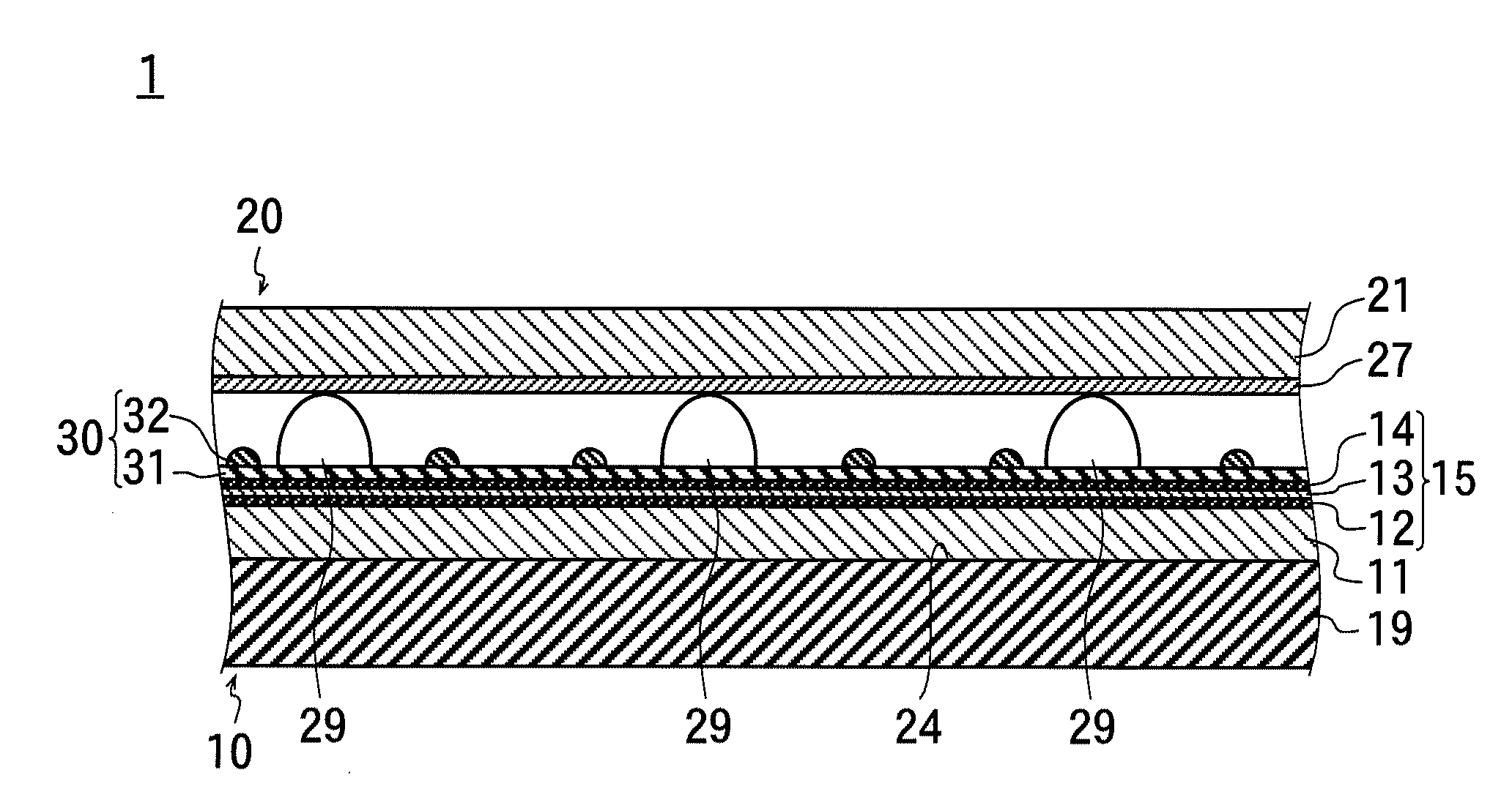
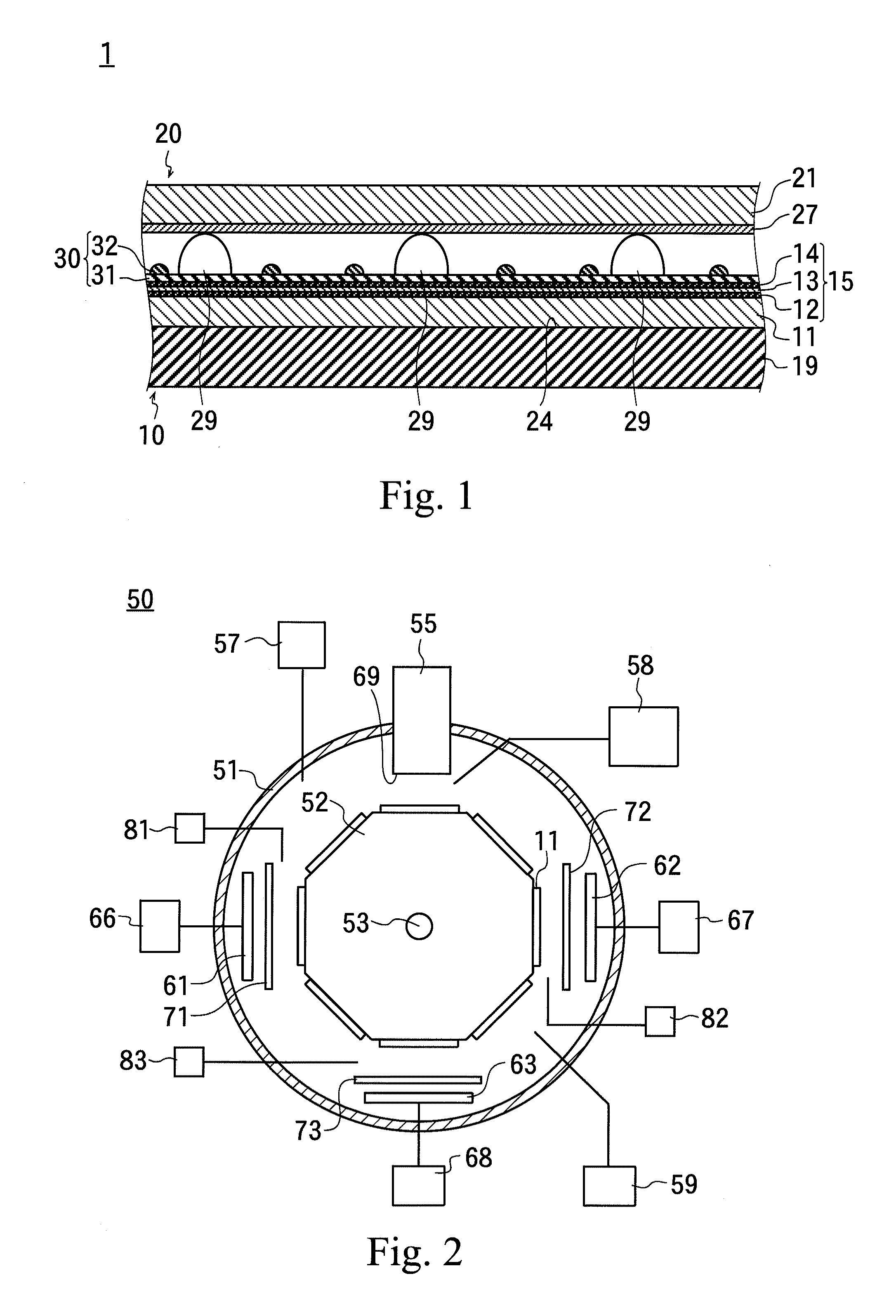
[0118]The object to be processed was taken out from the film forming apparatus 50, and carried into a vacuum chamber of the sputtering apparatus. A metal target 61 made of Nb was arranged in the vacuum chamber, and the object to be processed was faced toward the metal target 61. The vacuum chamber was evacuated to vacuum, and an island-shaped thin film of the Nb oxide (NbxOy) was formed as protective bodies 32 by sputtering the metal target 61, while both a reactive gas (oxygen gas) and a sputtering gas were being fed into a space between the metal target 61 and the object to be processed (Reactive sputtering). The film thickness of the NbxOy thin film was calculated to be 0.5 nm based on the film forming time.
example 2
[0119]The rotary body 52 was rotated in the state that the object to be processed was attached to the rotary body 52 of the film forming apparatus 50; the metal target 61 made of Nb was sputtered; the reactive gas of the oxygen gas was plasmatized; and an island-shaped NbxOy thin film was formed as protective bodies 32 by the above-mentioned metal mode. The film thickness of the NbxOy thin film was calculated to be 0.5 nm based on the film forming time.
example 3
[0120]The object to be processed was taken out from the film forming apparatus 50, and carried into the vacuum chamber of the sputtering apparatus. While the vacuum chamber was being evacuated to vacuum, an atomic layer (Nb atomic layer) was formed in a scattered fashion on a surface of the transparent conductive film 31 by introducing an Ar gas as a sputtering gas into the vacuum chamber and sputtering the metal target 61 made of Nb inside the vacuum chamber.
[0121]Next, while the reactive gas of the oxygen gas was being introduced into the vacuum chamber, protective bodies 32 made of the Nb atomic layer and a NbxOy protecting film covering the Nb atomic layer were formed by irradiating an ion beam toward the object to be processed from the ion gun. The film thickness of the protective body was calculated to be 0.5 nm based on the film forming time.
PUM
 Abstract
Description
Claims
Application Information


