

ESD protection structure
a protection structure and electronic shield technology, applied in the direction of circuit arrangements, semiconductor devices, electrical equipment, etc., can solve the problems of esd, which is a continuing problem in the integrated circuit, and the complexity of esd protection
- Summary
- Abstract
- Description
- Claims
- Application Information
AI Technical Summary
Problems solved by technology
Method used
Image

Examples
Embodiment Construction
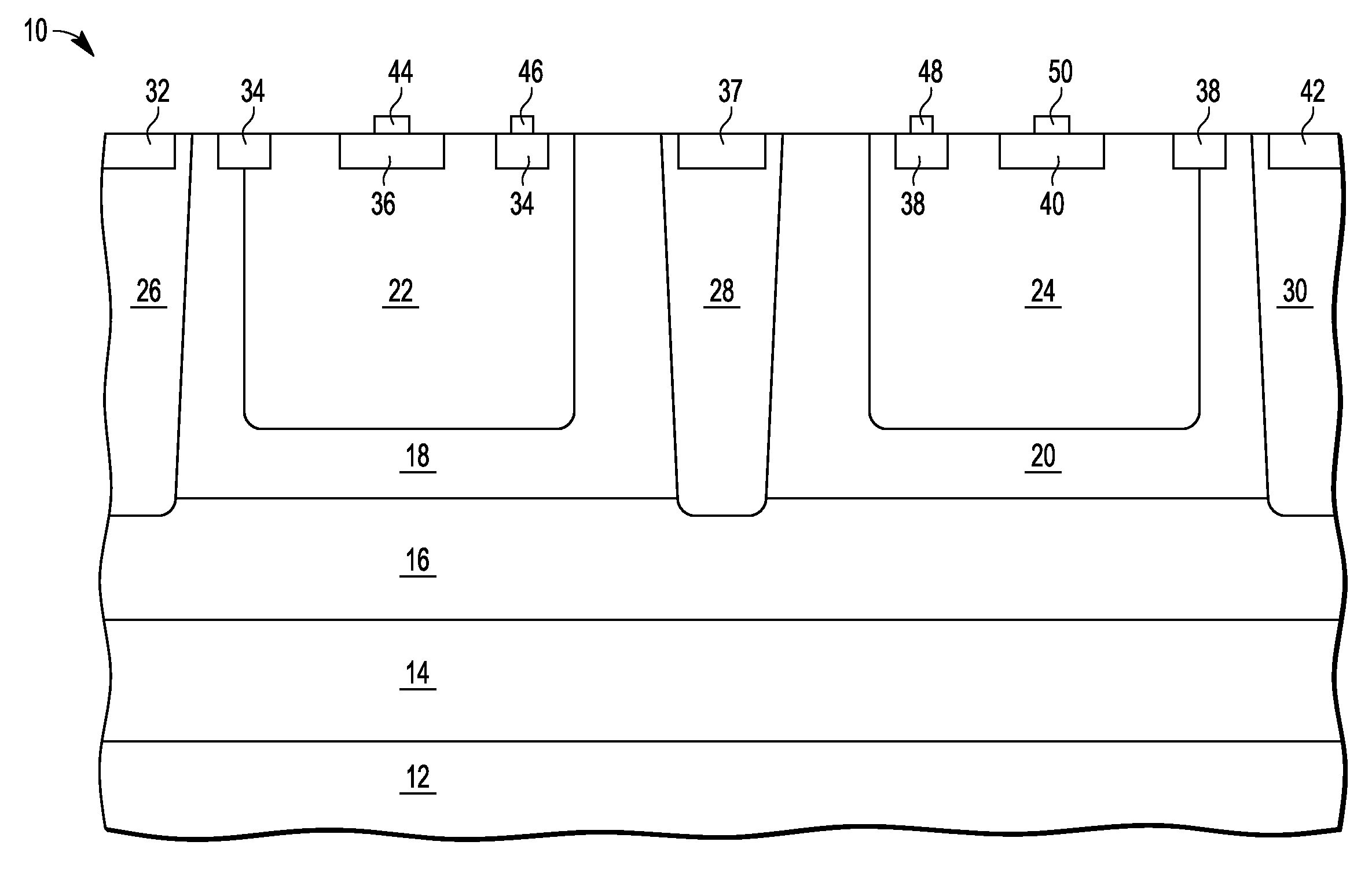
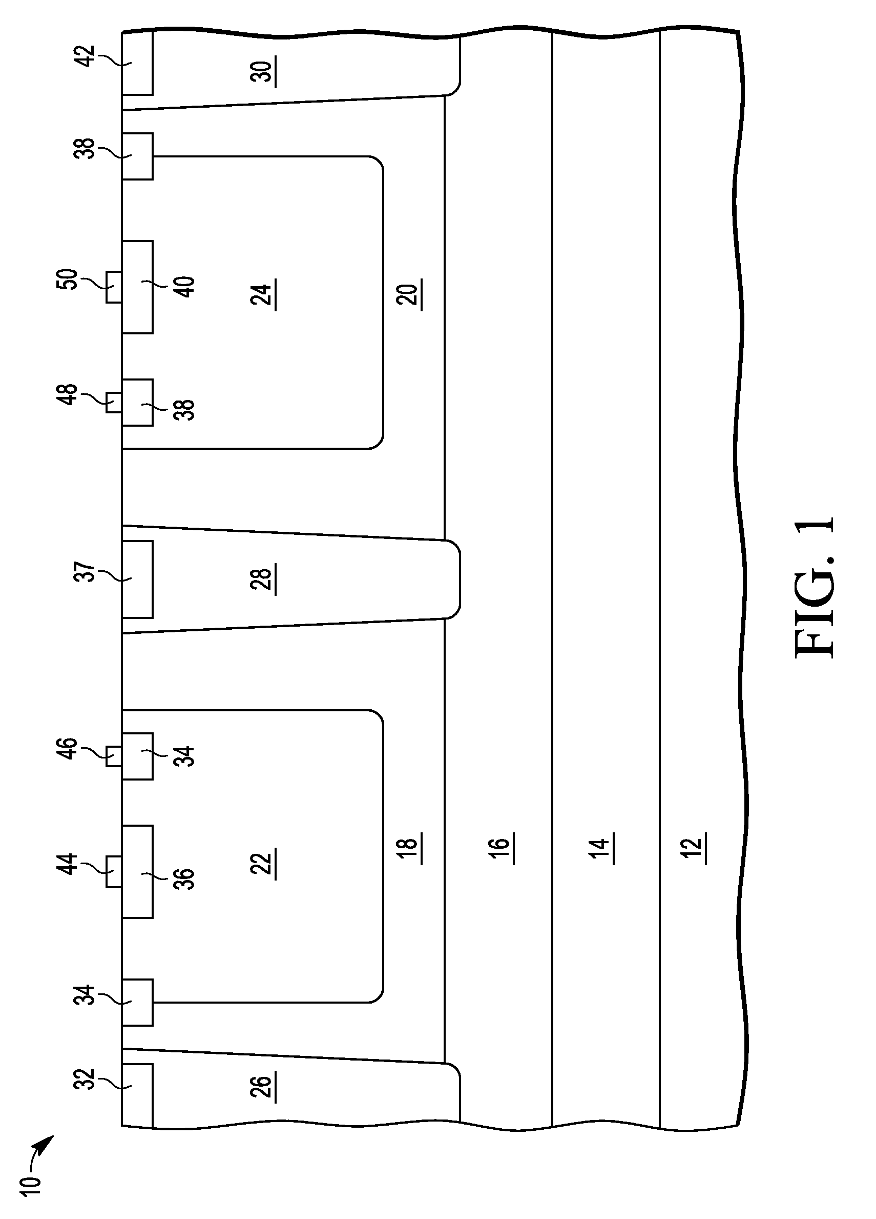
[0010]In one aspect, an ESD protection structure that is coupled to an I / O pad includes an efficient way of providing ESD protection for both positive and negative ESD events. A large commonality of elements is achieved in providing protection for both positive and negative ESD events while achieving ESD protection for the I / O pad. This is better understood by reference to the following specification and drawings.
[0011]Shown in FIG. 1 is a semiconductor device 10 comprising a substrate 12 that has had an epitaxial layer grown over it. Substrate 12 may be of silicon heavily doped to P type and the epitaxial layer may also be silicon. Formed in the epitaxial layer is a P layer 14 that is lightly doped over substrate 12, an N layer 16 that is heavily doped over P layer 14, connection regions 26, 28, and 30 of N type that are heavily doped and extend from a top surface of semiconductor device 10 to penetrate into N layer 16, a P region 18 from the top surface to N layer 16 and between c...
PUM
 Abstract
Description
Claims
Application Information