

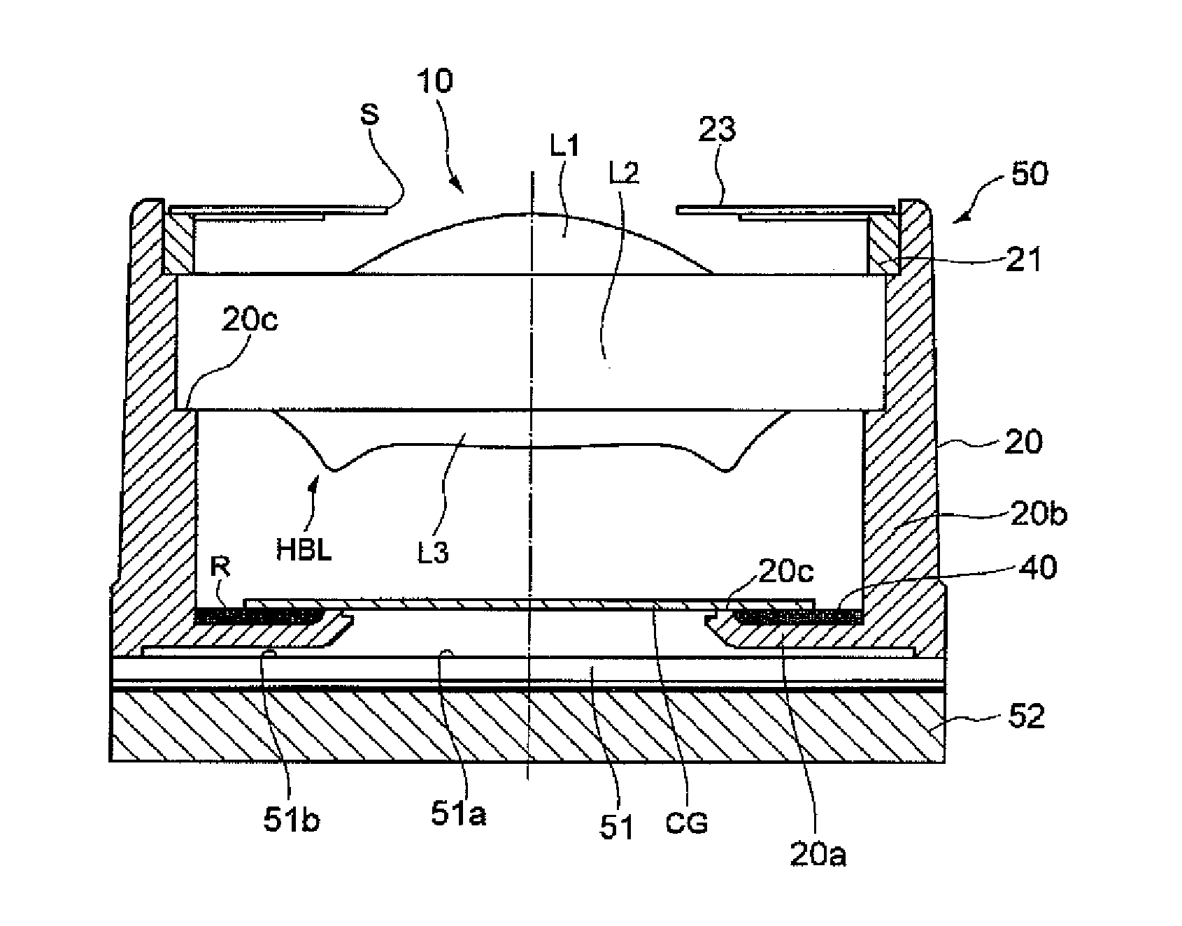
Imaging Lens, Imaging Device, and Portable Terminal
a technology of imaging device and lens, which is applied in the field of imaging lens, can solve the problems of deteriorating optical performance, inability to meet the requirement for a lower-cost imaging device, and expensive lenses, etc., and achieves compact configuration, high-volume production, and excellent aberration performance.
- Summary
- Abstract
- Description
- Claims
- Application Information
AI Technical Summary
Benefits of technology
Problems solved by technology
Method used
Image

Examples
example 1
[0147]Table 1 shows the lens data in the Example 1. In the following Tables, E (e.g., 2.5E-03) will be used to express the power of 10 (e.g., 2.5×10⁻³).
TABLE 1f = 1.48 mmfB = 0.89 mmENTP = 0.00 mmEXTP = −1.00 mmF = 2.82Y = 1.76 mmH1 = −0.34 mmH2 = −0.55 mmSurfaceRD*1number(mm)(mm)Ndνd(mm)1 (stop)∞0.200.272*1.0430.181.5350052.00.483∞0.401.5231055.00.484∞0.121.5350052.00.505*−2.5240.200.516∞0.58Aspherical surface coefficient2nd surface5th surfaceK =−3.0000E+01K =−1.3790E+01A4 = 3.4052E+00A4 = 8.4445E−01A6 =−2.1290E+01A6 =−2.5681E+00A8 = 1.0127E+02A8 = 2.6411E+01A10 =−2.6707E+02A10 =−9.7867E+01A12 = 2.9546E+02A12 = 1.5434E+02*1; Effective radius
[0148]The values for conditional expressions (1) through (4) in the first Example are as follows:
f1 / f3=0.413 Conditional expression (1)
S / f=0.257 Conditional expression (2)
ν1−ν3=0 Conditional expression (3)
dc / f=0 Conditional expression (4)
[0149]FIG. 6 is a cross section of a first Example, and FIG. 7 is an aberration diagram representing the ...
example 2
[0152]Table 2 shows the lens data in the second Example.
TABLE 2f = 1.41 mmfB = 0.63 mmENTP = 0.00 mmEXTP = −1.24 mmF = 2.82Y = 1.76 mmH1 = −0.38 mmH2 = −0.73 mmSurfaceRD*1number(mm)(mm)Ndνd(mm)1 (stop)∞0.200.252*1.0570.181.5350052.00.483∞0.501.5231055.00.494∞0.041.5350052.00.535*−2.0160.200.616∞0.301.5168064.20.697∞Aspherical surface coefficient2nd surface5th surfaceK =−7.1129E+00K =−4.8465E+00A4 = 1.1602E+00A4 = 7.2316E−01A6 = 1.8143E+00A6 =−4.9278E−01A8 =−4.6744E+01A8 = 7.5737E+00A10 = 2.3359E+02A10 =−1.7379E+01A12 =−3.8037E+02A12 = 2.0851E+01*1; Effective radius
[0153]The values for conditional expressions (1) through (4) in the second Example are as follows:
f1 / f3=0.524 Conditional expression (1)
S / f=0.268 Conditional expression (2)
ν1−ν3=0 Conditional expression (3)
dc / f=0.213 Conditional expression (4)
[0154]FIG. 8 is a cross section of a second Example. FIG. 9 is an aberration diagram for the imaging lens in the second Example. FIG. 9a is a diagram representing the spherical ab...
example 3
[0156]Table 3 shows the lens data in the third Example.
TABLE 3f = 1.46 mmfB = 0.55 mmENTP = 0.00 mmEXTP = −1.02 mmF = 2.82Y = 1.685 mmH1 = −0.13 mmH2 = −0.87 mmSurfaceRD*1number(mm)(mm)Ndνd(mm)1 (stop)∞0.080.262*0.9290.081.5737029.00.343∞0.521.6504059.40.344∞0.081.5737029.00.405*−6.4630.160.426∞0.501.5168064.20.497∞0.65Aspherical surface coefficient2nd surface5th surfaceK = 4.9179E+00K =−4.8000E+02A4 =−6.2160E−01A4 = 8.3206E−01A6 = 9.7587E+00A6 = 1.1917E−01A8 =−1.8666E+02A8 = 5.7674E+00A10 = 8.6212E+02A10 = 1.7335E+01A12 =−3.3169E+03A12 =−1.3056E+02*1; Effective radius
[0157]The values for conditional expressions (1) through (4) in the third Example are as follows:
f1 / f3=0.144 Conditional expression (1)
S / f=0.109 Conditional expression (2)
ν1−ν3=0 Conditional expression (3)
dc / f=0.342 Conditional expression (4)
[0158]FIG. 10 is a cross section of the third Example. FIG. 11 is an aberration diagram for the imaging lens in the third Example. FIG. 11a shows the spherical aberration, FIG....
PUM
 Abstract
Description
Claims
Application Information