
Image pickup lens, image pickup apparatus, mobile terminal, and manufacturing method of image pickup lens

A camera lens and lens technology, applied in optics, instruments, electrical components, etc., can solve problems such as the difficulty of ambiguity

Inactive Publication Date: 2014-06-18
KONICA MINOLTA OPTO
View PDF7 Cites 0 Cited by
  • Summary
  • Abstract
  • Description
  • Claims
  • Application Information

AI Technical Summary

Problems solved by technology

However, it is becoming more and more difficult to achieve the compatibility of such imaging lenses as the demands for the miniaturization of such imaging lenses and the mass production of portable terminals are increasing.

Method used

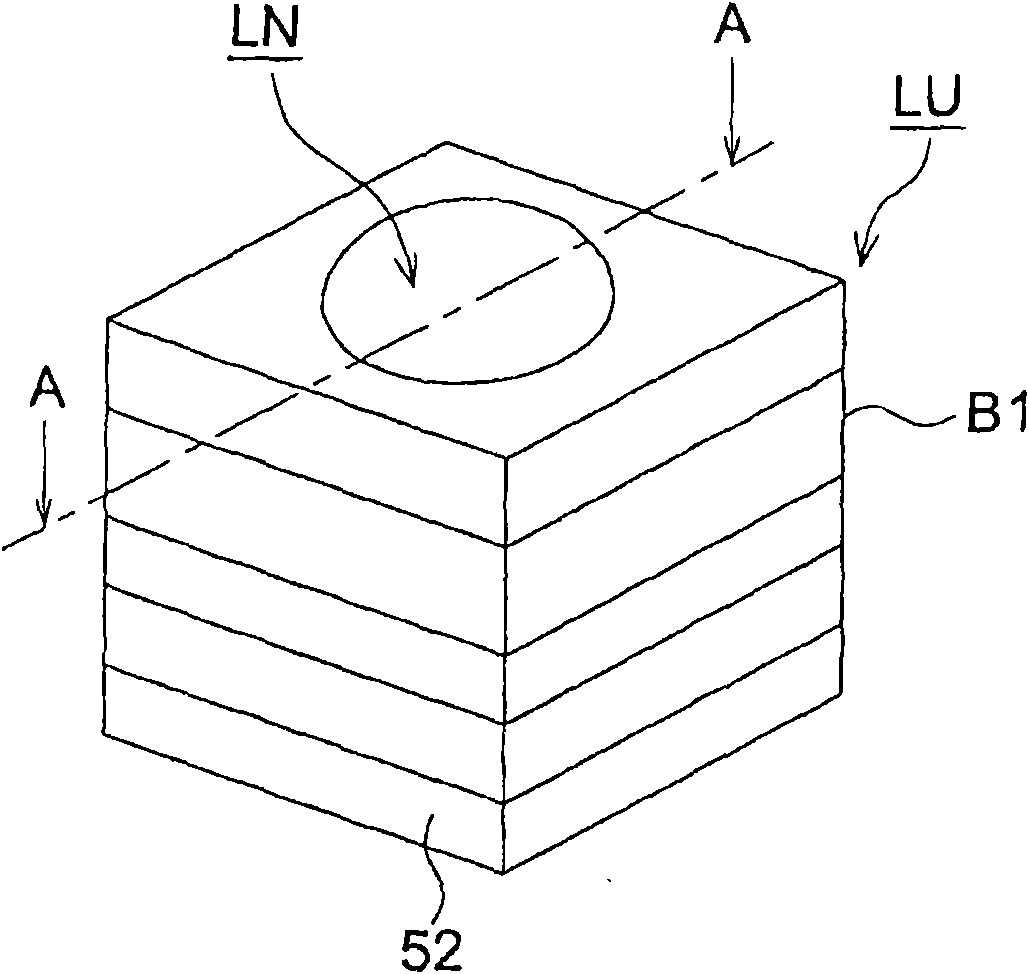
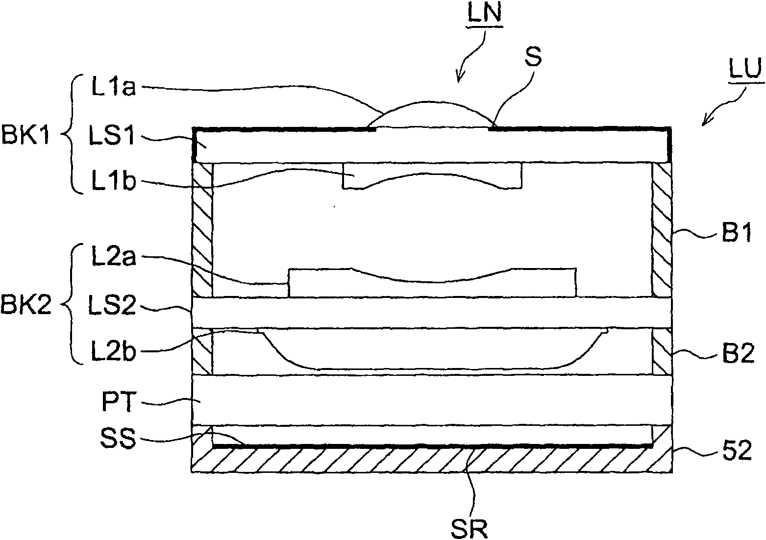
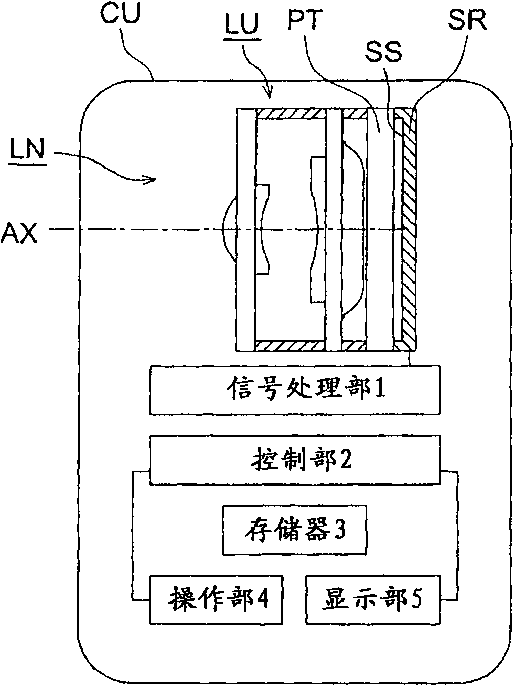

Image

  • Image pickup lens, image pickup apparatus, mobile terminal, and manufacturing method of image pickup lens
  • Image pickup lens, image pickup apparatus, mobile terminal, and manufacturing method of image pickup lens
  • Image pickup lens, image pickup apparatus, mobile terminal, and manufacturing method of image pickup lens

Examples


Embodiment 1

[0217] The system data is as follows:

[0218] f=2.98mm

[0219] fB=0.16mm

[0220] F=2.8

[0221] 2Y=3.5mm

[0222] ENTP=0.22mm

[0223] EXTP=-1.80mm

[0224] H1=-1.33mm

[0225] H2=-2.82mm.

[0226] The surface data is as follows:

[0227]Surface No. R(mm) D(mm) Nd vd Effective Radius(mm)

[0228] 1(*) 0.825 0.30 1.513 55 0.56

[0229] 2(aperture) ∞ 0.39 1.470 65 0.51

[0230] 3 ∞ 0.07 1.590 30 0.50

[0231] 4(*) 2.307 0.41 0.50

[0232] 5(*) -2.856 0.14 1.570 35 0.58

[0233] 6 ∞ 0.69 1.470 65 0.78

[0234] 7 ∞ 0.49 1.570 35 1.31

[0235] 8(*) 9.805 0.10 1.39

[0236] 9 ∞ 0.50 1.516 64 1.59

[0237] 10 ∞ 0.16 1.71

[0238] The aspheric coefficients are as follows:

[0239] side 1

[0240] K=0.24110E-01, A4=-0.76992E-02, A6=0.22116E+00, A8=-0.89518E+00, A10=0.76286E-01, A12=0.12557E+01, A14=0.14692E+02 , A16=-0.81966E+01, A18=-0.47815E+02, A20=-0.10647E+02

[0241] side 4

[0242] K=0.11699E+02, A4=0.15488E+00, A6=-0.22486E+00, A8=0.54011E+00, A10=0.941...

Embodiment 2

[0264] The system data is as follows:

[0265] f=2.93mm

[0266] fB=0.07mm

[0267] F=2.78

[0268] 2Y=3.5mm

[0269] ENTP=0.57mm

[0270] EXTP=-1.75mm

[0271] H1=-1.22mm

[0272] H2=-2.86mm.

[0273] The surface data is as follows:

[0274] Surface No. R(mm) D(mm) Nd vd Effective Radius(mm)

[0275] 1(*) 0.783 0.33 1.518 57 0.57

[0276] 2 ∞ 0.30 1.520 62 0.52

[0277] 3(aperture) ∞ 0.06 1.572 35 0.40

[0278] 4(*) 1.814 0.35 0.44

[0279] 5(*) -3.460 0.11 1.572 35 0.57

[0280] 6 ∞ 1.10 1.520 62 0.69

[0281] 7 ∞ 0.41 1.572 35 1.37

[0282] 8(*) 9.576 0.10 1.45

[0283] 9 ∞ 0.50 1.470 65 1.60

[0284] 10 ∞ 0.07 1.72

[0285] The aspheric coefficients are as follows:

[0286] side 1

[0287] K=-0.30420E+00, A4=0.61331E-01, A6=0.52666E+00, A8=-0.63008E+00, A10=-0.56268E+00, A12=0.60414E+01

[0288] side 4

[0289] K=0.50116E+01, A4=0.30772E+00, A6=-0.15497E+01, A8=0.25529E+02, A10=-0.11225E+03, A12=0.26608E+03

[0290] side 5

[0291] K=-0.13614E+02, A4...

Embodiment 3

[0310] The system data is as follows:

[0311] f=3.04mm

[0312] fB=0.16mm

[0313] F=2.88

[0314] 2Y=3.5mm

[0315] ENTP=0.18mm

[0316] EXTP=-1.84mm

[0317] H1=-1.39mm

[0318] H2=-2.88mm.

[0319] The surface data is as follows:

[0320] Surface No. R(mm) D(mm) Nd vd Effective Radius(mm)

[0321] 1(*) 0.845 0.25 1.513 55 0.55

[0322] 2 ∞ 0.30 1.470 65 0.51

[0323] 3(aperture) ∞ 0.17 1.610 29 0.50

[0324] 4(*) 2.231 0.49 0.50

[0325] 5(*) -4.276 0.17 1.572 35 0.63

[0326] 6 ∞ 0.88 1.470 65 0.81

[0327] 7 ∞ 0.33 1.700 36 1.39

[0328] 8(*) 8.194 0.10 1.46

[0329] 9 ∞ 0.50 1.516 64 1.58

[0330] 10 ∞ 0.16 1.70

[0331] The aspheric coefficients are as follows:

[0332] side 1

[0333] K=-0.18642E-01, A4=0.42482E-01, A6=-0.11195E+00, A8=0.13865E+01, A10=-0.52066E+01, A12=0.89294E+01

[0334] side 4

[0335] K=0.27654E+01, A4=0.31830E-01, A6=0.42787E+01, A8=-0.33891E+02, A10=0.14295E+03, A12=-0.18868E+03

[0336] side 5

[0337] K=-0.16316E+02, A4...


PUM


Abstract

An image pickup lens includes a first lens block with a positive refractive power, a second lens block with a negative refractive power, and an aperture stop. The first lens block includes a first lens substrate, and lens portions 1a and 1b arranged on the first lens substrate. The lens portions 1a and 1b are different from the first lens substrate in at least one of a refractive index and an Abbe number. The second lens block includes a second lens substrate, and lens portions 2a and 2b arranged on the second lens substrate. The lens portions 2a and 2b are different from the second lens substrate in at least one of a refractive index and an Abbe number. The image pickup lens satisfies predetermined conditions relating to a refractive index of the lens portion 2b, and composite thicknesses of the first lens block and the second lens block.

Description

technical field [0001] The present invention relates to an imaging lens for an imaging device, wherein the imaging device is equipped with a solid-state imaging element such as a CCD (Charge Coupled Devices) type image sensor, a CMOS (Complementary Metal-Oxide Semiconductor) type image sensor, etc. An imaging lens using a wafer-scale lens optical system suitable for mass production, an imaging device equipped with the imaging lens, a portable terminal equipped with the imaging device, and a method of manufacturing the imaging lens. Background technique [0002] In recent years, portable terminals of thin electronic devices such as mobile phones and PDAs (Personal Digital Assistants) have been equipped with small and thin camera devices, thereby realizing mutual transmission of audio and image information with remote areas. [0003] The imaging element in the above imaging device uses a CCD type image sensor or a CMOS type image sensor. Recently, with the advancement of high...

Claims


Application Information

Patent Timeline
Patent Type & Authority Patents(China)
IPC IPC(8): G02B13/00G02B27/00G02B1/04
CPCG02B27/0025H01L27/14618H01L27/14625H01L27/14685H01L2924/0002H01L2924/00B82Y20/00G02B13/00G02B13/18
Inventor 佐藤正江川崎贵志
Owner KONICA MINOLTA OPTO
Learn More