Method of fabricating solar cell chips

a technology of solar cells and solar energy, applied in the field of solar cells, can solve the problems of limiting the widespread use of solar cells, the relative high cost of fabricating solar cells,

Inactive Publication Date: 2010-12-02
INT BUSINESS MASCH CORP
View PDF15 Cites 6 Cited by
  • Summary
  • Abstract
  • Description
  • Claims
  • Application Information

AI Technical Summary

Problems solved by technology

The relatively high cost of fabricating solar cells has seriously limited the widespread use of solar cells.

Method used


Image

  • Method of fabricating solar cell chips
  • Method of fabricating solar cell chips
  • Method of fabricating solar cell chips

Examples


Embodiment Construction

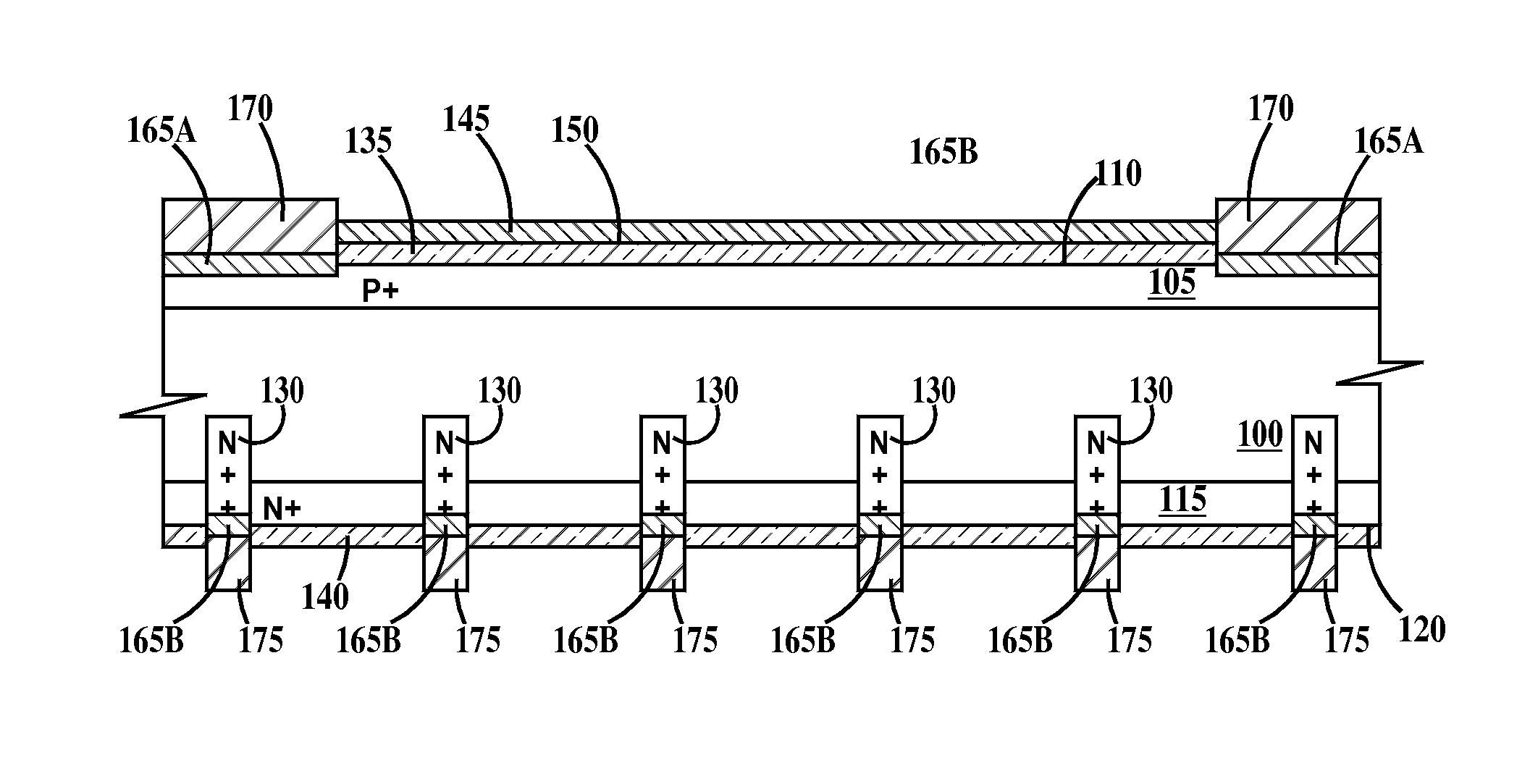
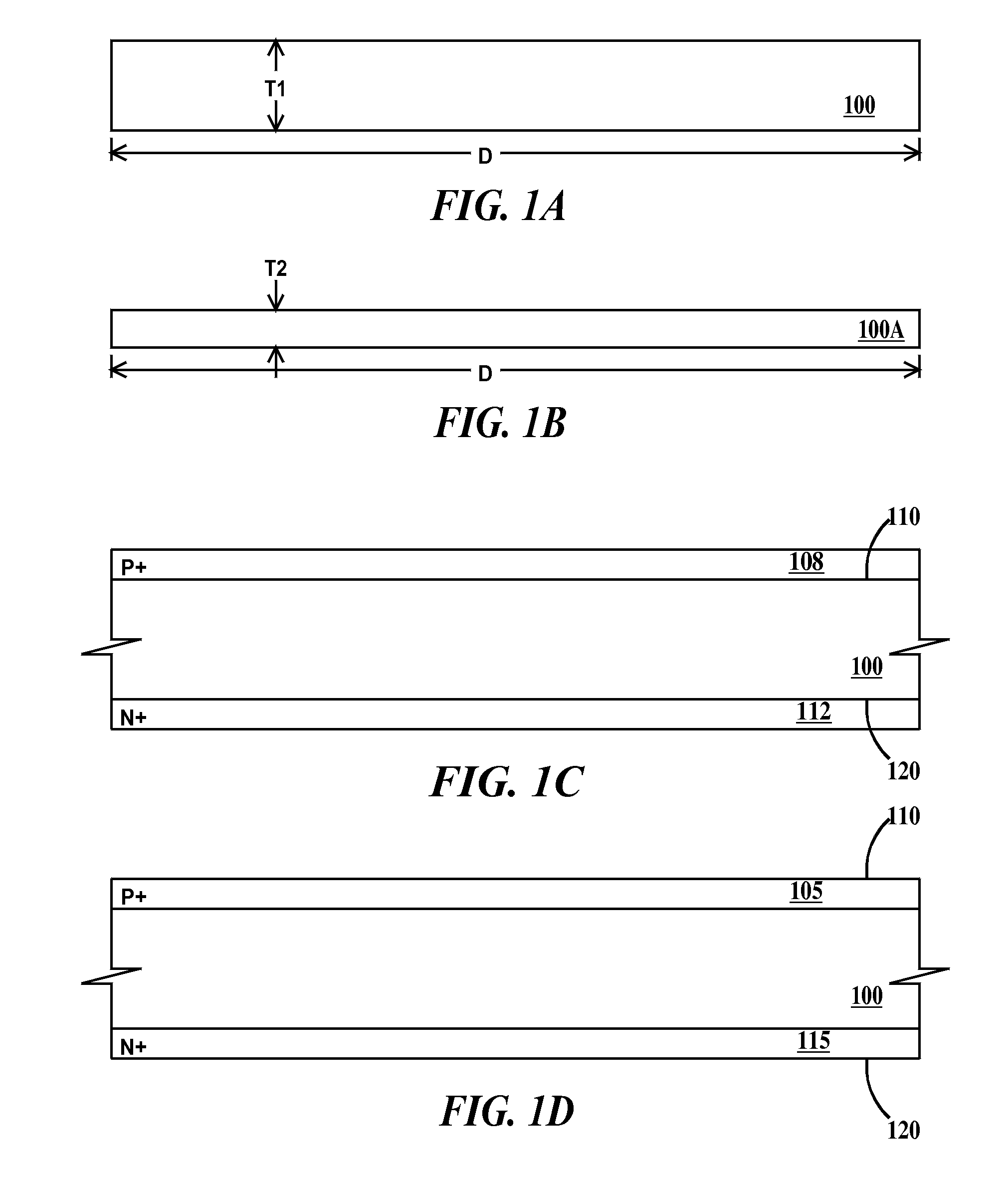
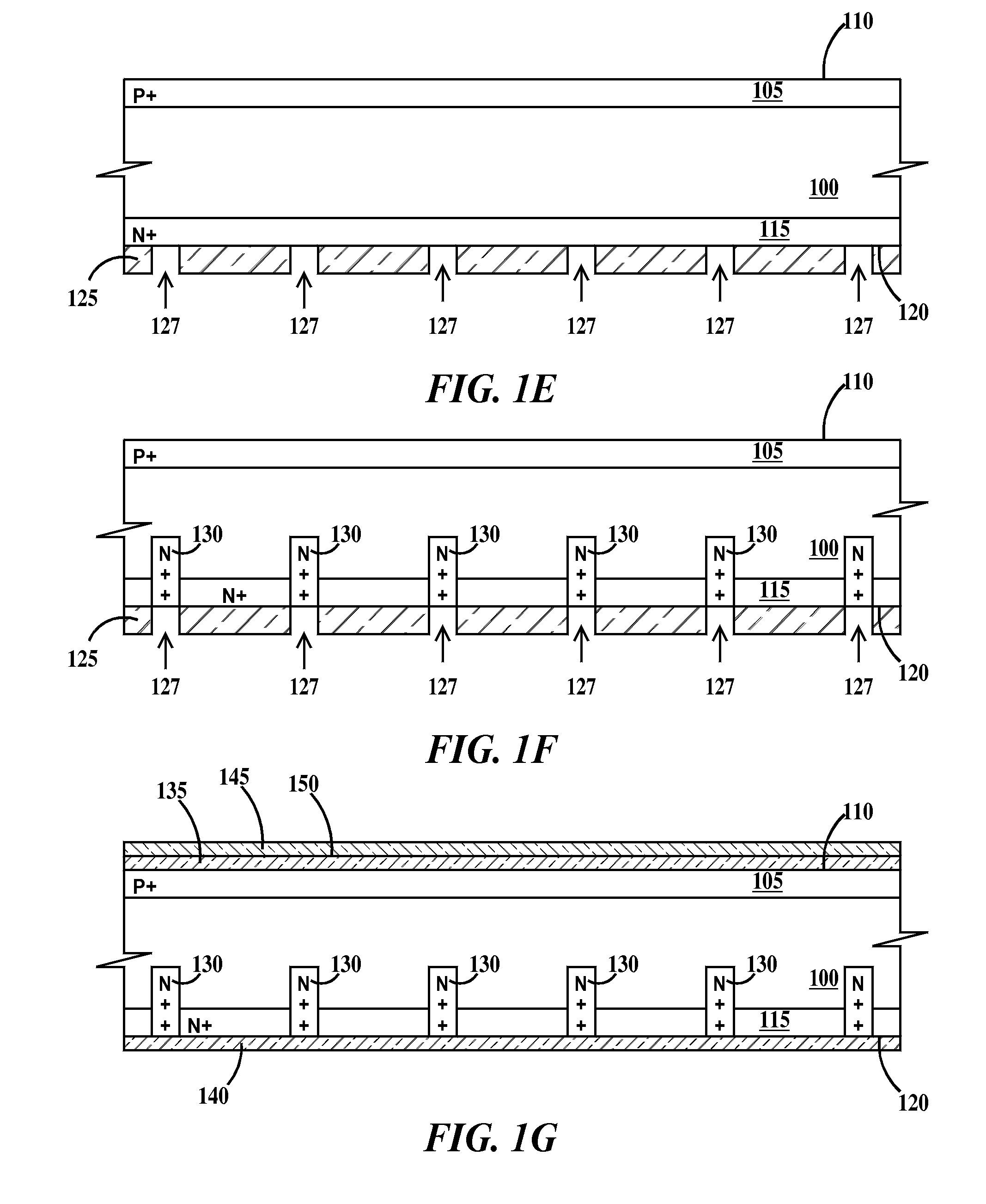
[0011]FIGS. 1A through 1J are cross-sectional drawings illustrating fabrication of a solar cell according to embodiments of the present invention. Generally, integrated circuit chips are fabricated using semiconductor substrates that are thin disc shaped substrates called wafers. The terms substrate and wafer may be used interchangeably herein. An integrated circuit chip is defined as a solid-state device including transistors (e.g., field effect and / or bipolar transistors) forming logic and / or memory circuits. The logic and / or memory circuits may be analog or digital.

[0012]In FIG. 1A, a bulk single-crystal silicon substrate 100 has a thickness T1 and a diameter D. In one example, D is about 300 mm and T1 is about 700 microns. In FIG. 1B, substrate 100 of FIG. 1A has optionally been thinned to a thickness T2. In one example T2 is about 300 microns. In one example T2 is less than 700 microns. In one example, T2 is less than about 700 microns and not less than about 300 microns. In on...


PUM


Abstract

A method of fabricating solar cell chips. The method includes creating an integrated circuit chip process route for fabricating integrated circuit chips using integrated circuit wafers in an integrated circuit fabrication facility; creating a solar cell process route for fabricating solar cells using solar cell wafers in the integrated circuit fabrication facility; releasing integrated circuit chip wafers and solar cell wafers into tool queues of tools of the an integrated circuit fabrication facility; and processing the solar cell wafers on at least some tools of the integrated circuit fabrication facility used to process the integrated circuit wafers. Also the process used to fabricate the solar cell chips.

Description

CROSS REFERENCE TO RELATED APPLICATION(S)[0001]This application is a division of application Ser. No. 12 / 189,911, filed Aug. 12, 2008, now pending, which is hereby incorporated herein by reference.FIELD OF THE INVENTION[0002]The present invention relates to the field of solar cells; more specifically, it relates to a method of fabricating a solar cell.BACKGROUND OF THE INVENTION[0003]Solar cells or solar concentrators are semiconductor devices capable of generating electricity using the photovoltaic effect. The relatively high cost of fabricating solar cells has seriously limited the widespread use of solar cells. Accordingly, there exists a need in the art to mitigate the deficiencies and limitations described hereinabove.SUMMARY OF THE INVENTION[0004]One aspect of the present invention is a method, comprising: creating an integrated circuit chip process route for fabricating integrated circuit chips using integrated circuit wafers in an integrated circuit fabrication facility; cre...

Claims


Application Information

Patent Timeline
Patent Type & Authority Applications(United States)
IPC IPC(8): H01L31/18H01L21/027H01L21/283
CPCH01L31/02168H01L31/022425H01L31/022433H01L31/068H01L31/1804H01L31/1868Y02E10/547Y02P70/521Y02P70/50
Inventor EICKELMANN, HANS-JUERGENHAAG, MICHAELHOVEL, HAROLD J.KRAUSE, RAINER KLAUSSCHMIDT, MARKUSSHAO, XIAOYANSTEEN, STEVEN ERIK
Owner INT BUSINESS MASCH CORP
Why Eureka
Try Eureka