Carrier structure for mounting LED chips

a carrier structure and chip technology, applied in the direction of basic electric elements, electrical equipment, semiconductor devices, etc., can solve the problems of inability to carry a higher electric voltage, led is vulnerable in use, and cannot sustain abnormal electric current flow by, so as to avoid the cost hike of providing the led assembly and ensure the yield

Inactive Publication Date: 2010-12-09
YIWANG GROUP
View PDF4 Cites 11 Cited by
  • Summary
  • Abstract
  • Description
  • Claims
  • Application Information

AI Technical Summary

Benefits of technology

[0010]Accordingly, it is an object of the present invention to provide a carrier structure for mounting LED chips, by which the mounting surface of the LED chips can differ from that of other electronic elements; such that the aforesaid shuttering problem can be reduced to a minimum, a cost hike for providing the LED assembly can be avoided, and the yield thereof can be ensured.

Problems solved by technology

However, the LED is vulnerable in usage.
For example, the LED cannot sustain abnormal electric currents to flow by, and cannot afford to carry a higher electric voltage, either.
Nevertheless, it would degrade the illumination efficiency of the LED chip if both the LED chip and the protection circuit are constructed close to each other at the same bonding surface.
However, though the shuttering problem of the design in FIG. 1 might be resolved by the design of FIG. 2, yet the cost for this change would be considerable and yield of the package of FIG. 2 would be lower by compared to that of FIG. 1.

Method used


Image

  • Carrier structure for mounting LED chips
  • Carrier structure for mounting LED chips
  • Carrier structure for mounting LED chips

Examples


Embodiment Construction

[0025]The invention disclosed herein is directed to a carrier structure for mounting LED chips. In the following description, numerous details are set forth in order to provide a thorough understanding of the present invention. It will be appreciated by one skilled in the art that variations of these specific details are possible while still achieving the results of the present invention. In other instance, well-known components are not described in detail in order not to unnecessarily obscure the present invention.

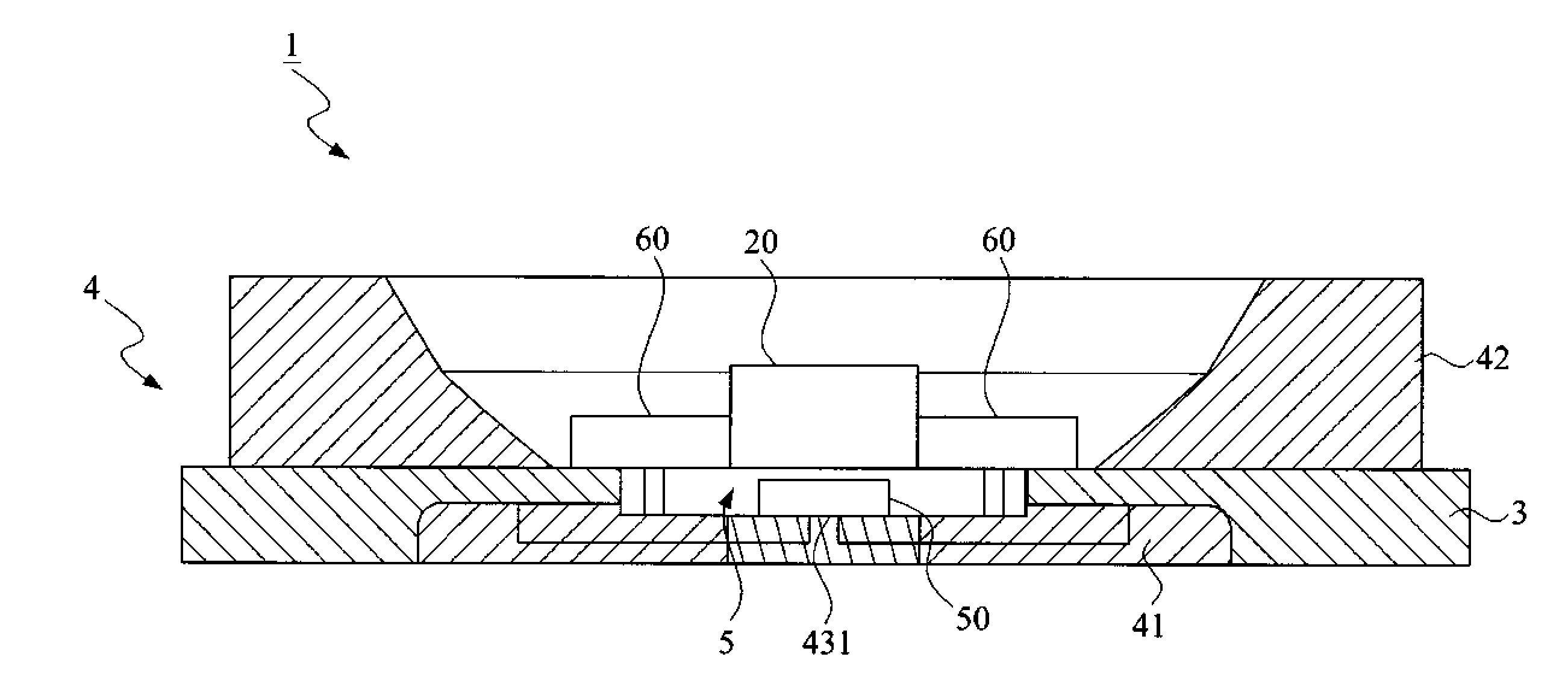
[0026]Referring now to FIG. 3, FIG. 4, FIG. 4A and FIG. 5, a perspective view of a first embodiment of the carrier structure 1 in accordance with the present invention, a perspective view of a base 4 of the carrier structure 1, a perspective view of leads 3 and a heat-dissipating block 43 of the carrier structure 1, and a cross-sectional view of FIG. 3 along line AA are shown, respectively. The carrier structure 1 includes at least one conductive lead 3 (six leads 3 shown...


PUM


Abstract

A carrier structure for mounting at least an LED chip includes at least a lead and a base. The LED chip housed inside the base is coupled parallel with an electronic element. The lead is connected electrically to the LED chip at one end, while another end is exposed to the atmosphere. The base encaving the lead further has a shallow accommodation room to mount the electronic element at a surface not the same with the surface that mounts the LED chip.

Description

[0001]This application claims the benefit of Taiwan Patent Application Serial No. 098210239, filed Jun. 9, 2009, the subject matter of which is incorporated herein by reference.BACKGROUND OF THE INVENTION[0002](1) Field of the Invention[0003]The invention relates to a carrier structure for mounting light-emitting diode (LED) chips, more particularly to the carrier structure that can provide superior shuttering protection for the LED chips mounted thereon.[0004](2) Description of the Prior Art[0005]Various merits of a typical LED product can be found; such as a long service life, a reduced size, high vibration resistance, low heat generation, low energy consumption and so on. Hence, the LED products are widely applied to various indicators and light sources for household and / or workplace usage. Recently, the trend in the LED technology is moving toward color and high-illumination products, and the application of the LEDs has been extended to large-scaled outdoor displaying, traffic s...

Claims


Application Information

Patent Timeline
Patent Type & Authority Applications(United States)
IPC IPC(8): H01L33/00
CPCH01L25/167H01L33/486H01L2224/48091H01L2224/48247H01L2924/3025H01L2924/00014H01L2924/00
Inventor LIAO, CHUN-YINGCHENG, CHING-CHI
Owner YIWANG GROUP
Why Eureka
Try Eureka