
Optical microstructure film and method for fabricating the same

a microstructure film and optical technology, applied in the field of optical microstructure films, can solve the problems of reducing the ability of shock absorption and anti-impact, affecting the performance of solar cells, so as to achieve the effect of reducing the moisture inside the package, reducing the cost of production, and reducing the risk of damag

Active Publication Date: 2015-02-10
ENTIRE TECH CO LTD
View PDF1 Cites 0 Cited by
  • Summary
  • Abstract
  • Description
  • Claims
  • Application Information

AI Technical Summary

Benefits of technology

The present invention is an optical microstructure film that can be used in packaging processes for various objects. The film has surface microstructure units that can reduce moisture inside the package, make demodeling in production easier, and increase production yield. Its use can also improve gas-expelling efficiency, ensure yield, and lower production cost. The design and usage of the film can be applied to various fields, not limited to the solar cell industry. The future and real market value of the invention shall be tremendous.

Problems solved by technology

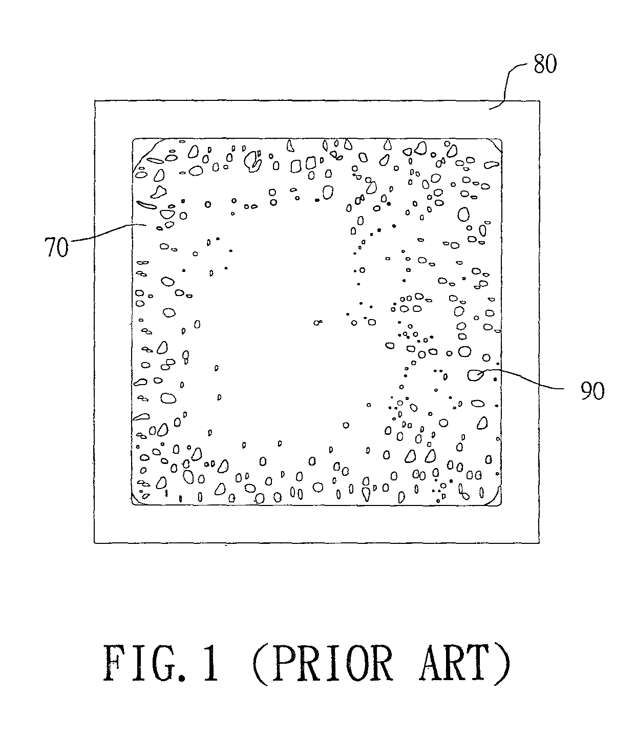
2. The existence of the gas voids 90 would sponge the optical film and thus reduce its capability in shock-absorbing and anti-impact.
As a result, the solar cell is vulnerable to breaks or damages while meeting foreign forcing.
However, if ventilation channels can't be formed between the microstructures 91 while the gluing resin is in a melted state, the result in gas-expelling would be far from being acceptable.
Further, the microstructures 91 can also lead to poor mold delamination upon the EVA optical film and a reduced yield of the EVA optical film 91.
However, in this disclosure, the problem in the disappearance of the ventilation channels during the melted state of the gluing material is yet to be resolved.

Method used


Image

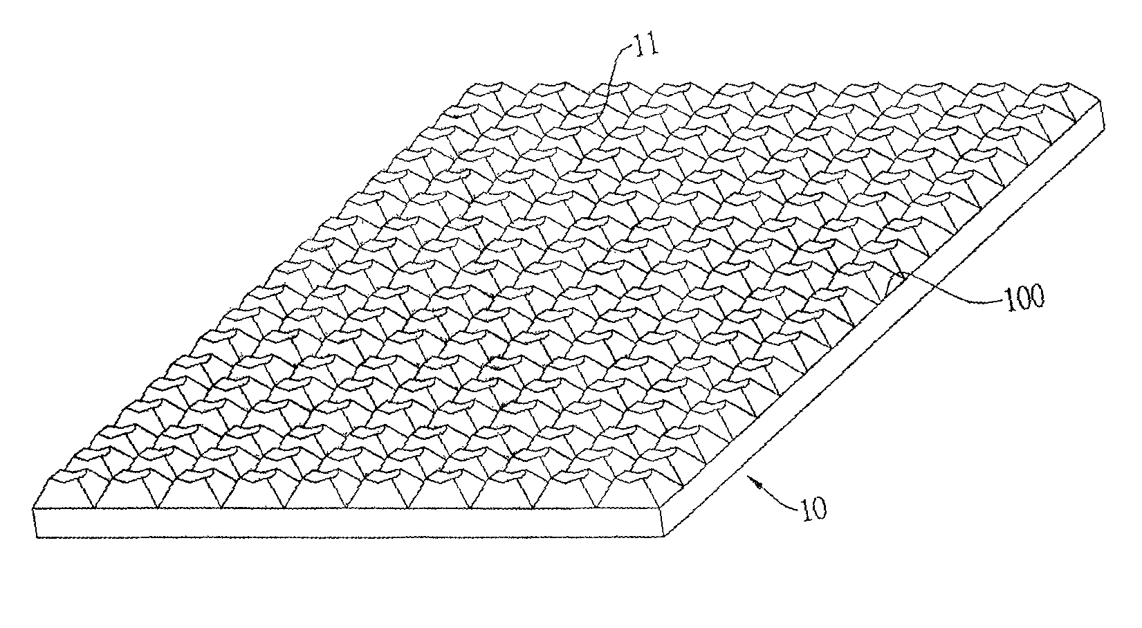
  • Optical microstructure film and method for fabricating the same
  • Optical microstructure film and method for fabricating the same
  • Optical microstructure film and method for fabricating the same

Examples


example 1

Testing for peeling strength of the EVA optical microstructure film in accordance with the present invention

[0060]A. Preparation of the film

[0061]1. Prepare a glass substrate by washing thoroughly with an isopropanol (IPA) solution and wiping off with a kimwipe;

[0062]2. Place the glass substrate on a release paper by flushing the glass substrate with the release paper at the respective lateral sides;

[0063]3. Cut a 1″×12″ piece of the EVA optical microstructure film of the present invention and place the piece of the film on the glass substrate;

[0064]4. Sandwich a piece of release paper between the glass substrate and the optical microstructure film, with the release paper extending ½″ (i.e. a half) into the spacing in between;

[0065]5. Prepare a 1″×12″ piece of TPT and place the TPT onto the EVA film to form a combination;

[0066]6. Place a release paper to completely cover the combination;

[0067]7. Heat to package the combination in accordance with a comprehensive testing spec; for exa...

example 2

Testing for gas-expelling efficiency of the EVA optical microstructure film in accordance with the present invention

[0078]A. Preparation of the test specimen

[0079]1. Sandwich a 10 cm×10 cm optical microstructure film between a 10 cm×10 cm front plate and a 10 cm×10 cm back plate, in which the front plate is a glass plate;

[0080]2. Use a vacuum laminating machine to adhere the front plate, the optical microstructure film and the back plate, under 150° C. for vacuuming 5-10 minutes, and then introduce an atmosphere pressure for 10-15 minutes to ensure the adhering and to obtain a specimen; and

[0081]3. Compute (A2 / A1)×100% and the gas-expelling efficiency 1−(A2 / A1)×100%, in which A1 is the total area of the specimen and A2 is the total area for the air bubbles on the specimen.

example 3

Testing Results of the Peeling Strength and the Gas-Expelling Efficiency of the EVA Optical Microstructure Film in Accordance with the Present Invention

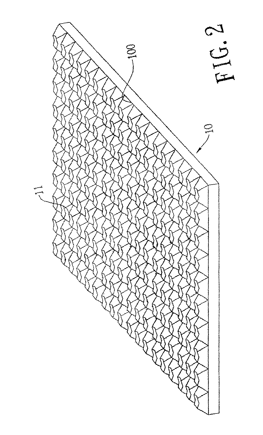
[0082]Referring to Table 1, Table 2 and Table 3, testing data for the films with different microstructure units 11, 11a and 11b are shown. In these tables, data for the gas-expelling efficiency, the peeling strength, the structural moduling ratio, the production yield (also the whole-span moduling ratio) and the machine number for production are included.

[0083]

TABLE 1Testing and Analysis results for the opticalmicrostructure film with triangular-cone microstructure units (n = 3)ItemGas-expellingPeelingStructuralPorosityGas-expellingefficiencystrengthmodulingMachineSpecimen(%)H2 / H1H3 / (H1 − H2)rate(mm3 / sec)(%)(N / cm)ratioYieldnumberMicostructure100.80.92008890⊚⊚⊚units:200.70.84009296⊚⊚⊚triangilar300.60.760095102⊚⊚⊚cone360.50.6720100116⊚⊚⊚(n = 3)400.450.5580098104⊚⊚⊚500.40.5100099108⊚⊚⊚600.30.4120096103⊚⊚⊚700.20.314009192ΔΔΔ800.10.216009...


PUM

PropertyMeasurementUnit
porosityaaaaaaaaaa
porosityaaaaaaaaaa
optical microstructureaaaaaaaaaa

Abstract

An optical microstructure film includes a base and multiple microstructure units. The base has at least a surface. The microstructure units are disposed in an array manner on the surface of the base. Each microstructure unit is formed to be a polygonal cone having the bottom face is attached to the surface of the base. The concave region is a surface part of a pseudo-spherical structure having a lower point on the microstructure unit. The distance from the lower point to the bottom face is defined as a second height, the sum of a radius of the spherical structure and the second height is defined as a first height, and the ratio of the second height to the first height is ranged from 0.1 to 0.8.

Description

BACKGROUND OF INVENTION[0001]1. Field of the Invention[0002]The invention is related to an optical microstructure film and a method for fabricating the optical microstructure film, and more particularly to the optical microstructure film applicable to solar cells. The optical microstructure film introduces special microstructures to reduce the formation of gas inside the solar cell so as to improve the yield in mold stripping during the manufacturing of the solar cells.[0003]2. Description of the Prior Art[0004]Referring to FIG. 1, it is shown that an optical film of a conventional solar cell is located tightly between a glass substrate 70 and a back plate 80. During a packaging process in the art, air bubbles or gas voids 90 are opt to be formed between the optical film and the glass substrate 70. Following disadvantages would prevail while meeting the gas voids 90.[0005]1. Possible moisture inside the gas voids 90 on the optical film would lead possible shortcut in electrical elem...

Claims


Application Information

Patent Timeline
Patent Type & Authority Patents(United States)
IPC IPC(8): B32B3/00B32B3/14B32B37/00B32B37/06B32B37/10F21V8/00G02B1/00G02B3/00G02B5/02G02B5/04H01L31/048H01L31/052
CPCB32B3/14B32B37/003B32B37/06B32B37/10G02B1/00G02B3/005G02B5/0215G02B5/045G02B6/0028H01L31/0481H01L31/0488H01L31/0522B32B2457/12Y02E10/52B32B27/06B32B27/306B32B2307/54B32B2551/00H01L31/0543Y10T428/163Y10T428/24479Y10T428/24628
Inventor CHEN, HSIN-YUANHSIEH, YU-YUNLIAO, CHENG-LUN
Owner ENTIRE TECH CO LTD
Learn More