Semiconductor device and manufacturing method thereof

a technology of semiconductor devices and manufacturing methods, which is applied in the field of flash devices, can solve the problems of increasing the manufacturing difficulty of semiconductor devices, advancing towards physical possible limits, and subsequent wet cleaning processes causing large torque to the gates, so as to ensure the yield of semiconductor devices, process flow optimization

Active Publication Date: 2022-02-10
SHANGHAI HUALI MICROELECTRONICS CORP
View PDF2 Cites 0 Cited by
  • Summary
  • Abstract
  • Description
  • Claims
  • Application Information

AI Technical Summary

Benefits of technology

[0034]According to the method for manufacturing a semiconductor device provided on one embodiment of the present disclosure, the process flow is optimized. Compared with the prior art, the interlayer dielectric layer is protected from being affected by the subsequent wet cleaning process, and the torque produced by the wet cleaning reagent on stacked film structures where the stacked gates are located is reduced, thereby avoiding the problem of collapse of the stacked gates. Meanwhile, since the side walls at the bottoms of the stacked gates are retained, the subsequent ion implantation process will not be significantly affected. According to the semiconductor device provided by another aspect of the present disclosure, the problem of collapse of the stacked gates is avoided, the interlayer dielectric layer can be protected, and the ion implantation is not affected, so the yield of the semiconductor device can be ensured.

Problems solved by technology

The manufacturing of semiconductor devices has thus become increasingly challenging and advanced towards physically possible limits.
However, because the oxide layer on the side walls has hydrophilic characteristic, the subsequent wet cleaning process produces a large torque to the gates.
Particularly, in the case where the sizes of gaps between adjacent gates are inconsistent, the difference in gap sizes on both sides of the gate will cause torque imbalance on two sides of the gate, thereby intensifying the impact of the torque on the gate itself.
This imbalanced surface tension is very likely to incline the gate structures, and even more seriously cause the problem of collapse of the gate structures.

Method used


Image

  • Semiconductor device and manufacturing method thereof
  • Semiconductor device and manufacturing method thereof
  • Semiconductor device and manufacturing method thereof

Examples


Embodiment Construction

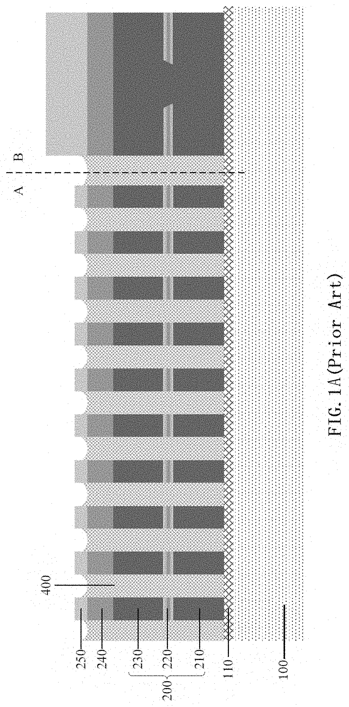
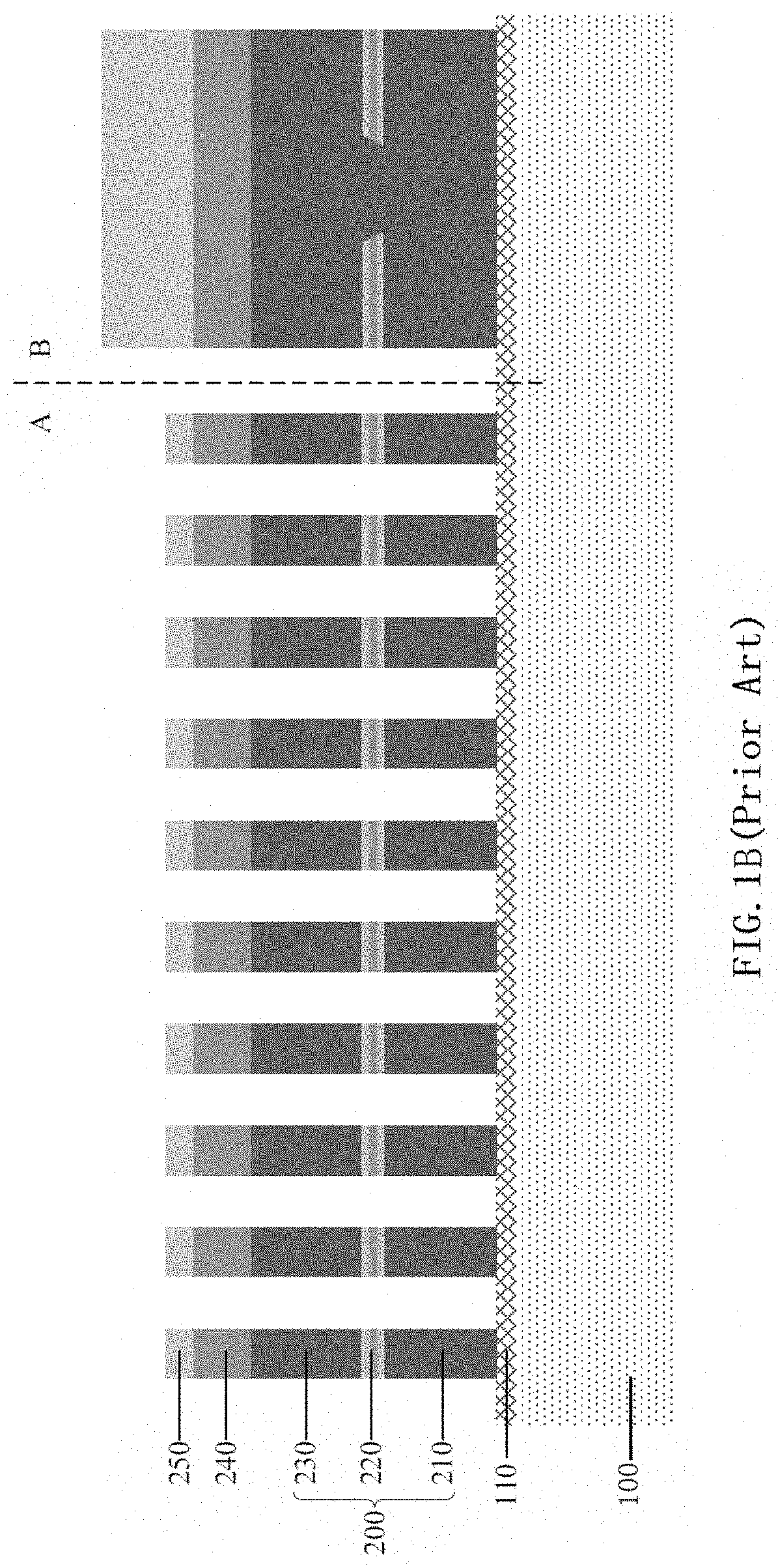
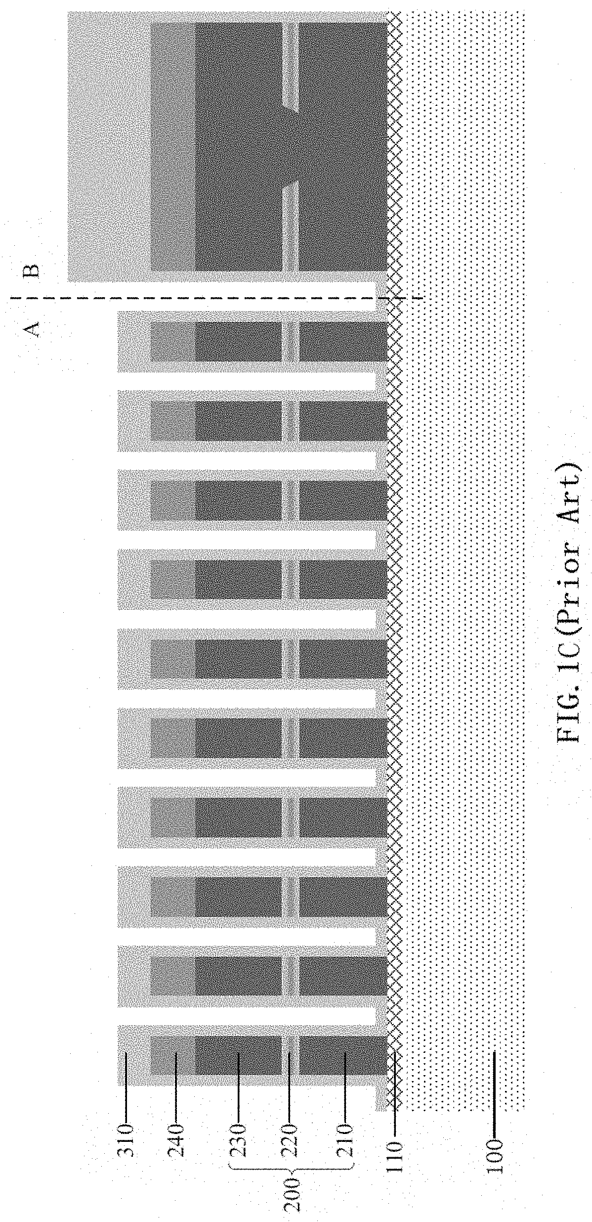
[0054]The following description is provided so that those skilled in the art can implement and use the present disclosure and combine it into a specific application background. Various modifications, and various uses in different applications will be readily apparent to those skilled in the art, and the general principles defined herein can be applied to a wide range of embodiments. Thus, the present disclosure is not limited to the embodiments given herein, but should be granted in the broadest scope of the principles and novel features disclosed herein.

[0055]Many specific details are set forth in the following detailed description to provide a thorough understanding of the present disclosure. However, it would be apparent to those skilled in the art that the practice of the present disclosure is not necessarily limited to these specific details. In other words, the well-known structures and devices are shown in the form of block diagrams without details to avoid obscuring the pres...


PUM

PropertyMeasurementUnit
height-width aspect ratiosaaaaaaaaaa
heightaaaaaaaaaa
dielectricaaaaaaaaaa

Abstract

The present disclosure provides a semiconductor device and a manufacturing method thereof. The manufacturing method comprises: providing a substrate comprising a storage region, forming stacked gates of storage transistors on the substrate; forming side walls on two sides of each stacked gate wherein the top surfaces of side walls are arranged to be lower than the top surfaces of the stacked gates; performing ion implantation in the storage region defined by the side walls; and performing an ashing process and a wet cleaning process using the side walls as protective layers of the stacked gates to remove a photoresist remaining after the ion implantation. The present disclosure further provides a semiconductor device formed according to the manufacturing method. According to the semiconductor device and the manufacturing method thereof, the problem of stacked gate collapse from the ion implantation process can be solved, thereby improving the yield.

Description

CROSS-REFERENCES TO RELATED APPLICATIONS[0001]This application claims the priority to Chinese patent application No. CN202010783067.2, filed on Aug. 06, 2020 and entitled “SEMICONDUCTOR DEVICE AND MANUFACTURING METHOD THEREOF”, the disclosure of which is incorporated herein by reference in its entirety.TECHNICAL FIELD[0002]The present disclosure relates to the field of semiconductor devices and manufacturing methods thereof, in particular, to a flash device and a manufacturing method thereof.BACKGROUND[0003]Since doctor Jack Kilby of Texas Instruments invented an integrated circuit in the early days, scientists and engineers have made many inventions and improvements on semiconductor devices and processes. In the past 50 years, the sizes of semiconductor transistors have been significantly reduced, which has led to a growing processing speed and continuously reduced power consumption. So far, the development of semiconductors roughly follows the Moore's law. The Moore's law generall...

Claims


Application Information

Patent Timeline
Patent Type & Authority Applications(United States)
IPC IPC(8): H01L21/28H01L29/788H01L29/66H01L27/11524H01L29/423
CPCH01L29/40114H01L29/788H01L29/42324H01L27/11524H01L29/66825H01L29/401H01L29/42364H10B41/35
Inventor XU, PENGKAIQIAO, FULONGREN, JIA
Owner SHANGHAI HUALI MICROELECTRONICS CORP
Why Eureka
Try Eureka