

Termination circuit and impedance matching device including the same
a technology of impedance matching and terminal circuit, which is applied in the direction of logic circuit coupling/interface arrangement, digital transmission, pulse technique, etc., can solve the problems of severe signal reflectance, general cause of impedance mismatching, and significant increas
- Summary
- Abstract
- Description
- Claims
- Application Information
AI Technical Summary
Benefits of technology
Problems solved by technology
Method used
Image

Examples
Embodiment Construction
[0035]Other objects and advantages of the present invention can be understood by the following description, and become apparent with reference to the embodiments of the present invention.
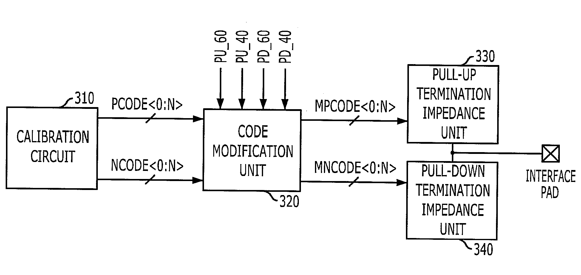
[0036]FIG. 3 is a block diagram of an impedance matching device in accordance with an embodiment of the present invention.
[0037]Referring to FIG. 3, the impedance matching device includes a calibration circuit 310, a code modification unit 320, and termination impedance units 330 and 340. The calibration circuit 310 generates impedance calibration codes PCODE and NCODE for modifying an impedance. The code modification unit 320 modifies the impedance calibration codes PCODE and NCODE according to impedance setting information PU_60, PU_40, PD_60 and PD_40 and outputs the modified impedance calibration codes MPCODE and NCODE. The impedance units 330 and 340 terminate an interface node (a node of a chip connected to an interface pad) with an impedance determined according to the modified impedance cali...
PUM
 Abstract
Description
Claims
Application Information