Chip packaging method and structure thereof

a technology of chip packaging and golden wires, applied in the direction of electrical apparatus, semiconductor devices, semiconductor/solid-state device details, etc., can solve the problems of wasting golden wires and too long length of connecting golden wires, and achieve the effects of saving metal wire cost, shortening the length of metal wires, and raising the transmission speed

Inactive Publication Date: 2010-12-16
KUN YUAN TECH
View PDF2 Cites 113 Cited by
  • Summary
  • Abstract
  • Description
  • Claims
  • Application Information

AI Technical Summary

Benefits of technology

[0011]A further object of the present invention is to provide a chip packaging structure, comprising a chip, at least a metal wire, a molding layer and a substrate. The chip includes an upper surface and a lower surface, the upper surface being provided with at least a bonding pad The at least a metal wire includes a first end and a second end, the first end being electrically connected to the at least a bonding pad of the chip. The molding layer is packaged to cover the chip and the at least a metal wire, the second end of the at least a metal wire being exposed to an upper surface of the molding layer. The substrate is attached onto the upper surface of the molding layer, a lower surface of the substrate including at least a circuit contact, which is correspondingly electrically coupled to the second end of the at least a metal wire. Thus, the chip packaging structure of the invention is capable of shortening the length of the metal wires in the internal part of the chip packaging structure so as to raise the transmission speed, save cost of the metal wires, and reduce the volume of the chip packaging body.
[0012]In addition, the chip packaging structure of the invention further comprises a carrier board, the lower surface of the chip being mounted on the carrier board. Functionally, the carrier board is able to facilitate the proceeding of the packaging process, other than protecting the chip. The chip packaging structure of the invention further comprises a fastening layer for fastening between the lower surface of the chip and the carrier board. The fastening layer is mainly for use in attaching the chip onto the carrier board. Further, in the chip packaging structure of the invention, the upper surface of the molding layer further comprises at least a metal pad, and the at least a circuit contact of the substrate is electrically connected to the second end of the at least a metal wire through the at least a metal pad. The metal pad of the invention not only can enlarge the size of the electrical contacting, but also can provide attaching the substrate to the molding layer. The at least a metal pad includes a tin-plated pad.

Problems solved by technology

Such an approach results is too long in length of the connecting golden wires 92, rendering waste of cost of the golden wires 92.

Method used


Image

  • Chip packaging method and structure thereof
  • Chip packaging method and structure thereof
  • Chip packaging method and structure thereof

Examples


Embodiment Construction

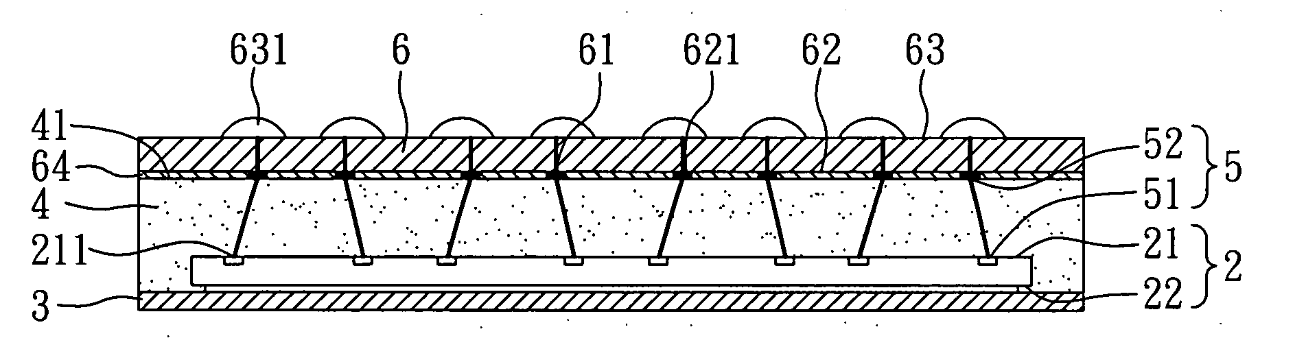
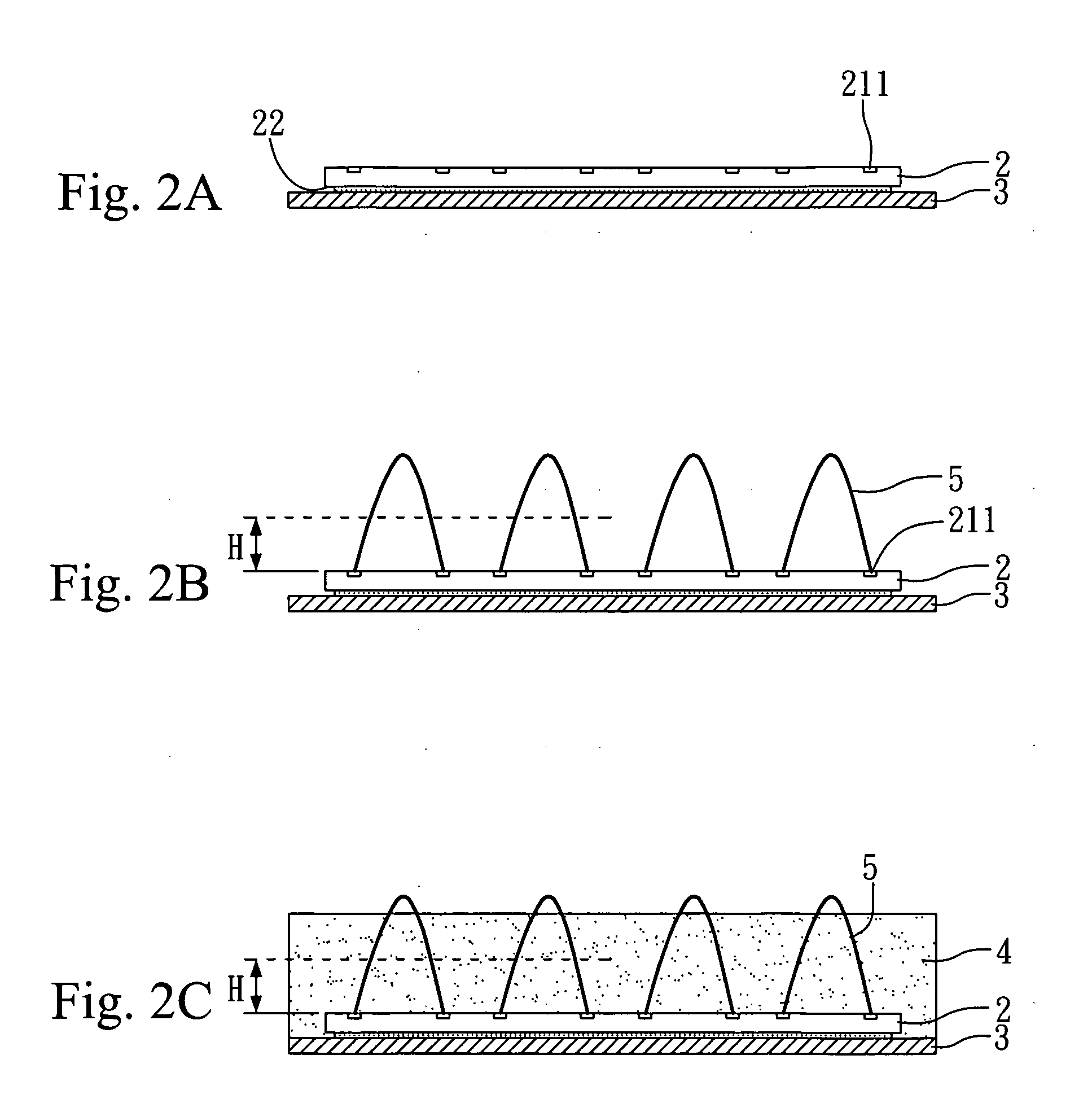
[0020]Please refer to FIGS. 2A to 2F together with FIG. 3. FIGS. 2A-2F are cross-sectional diagrams of each step for a chip packaging method of a preferred embodiment of the invention, and FIG. 3 is a flow chart of a preferred embodiment of the invention. Firstly, as shown in FIG. 2A, a chip 2 is provided, a plurality of bonding pads 211 are provided on an upper surface 21 thereof and a lower surface 22 of the chip 2 is mounted on a carrier board 3 (step A in FIG. 3). However, the carrier board 3 may be added in dependence of the condition or need and is mainly used for protecting the chip 2, while facilitating the proceeding of the packaging process.

[0021]Next, as shown in FIG. 2B, a plurality of metal wires 5 are connected out via bonding (step B in FIG. 3), and a middle part of each of the plurality of metal wires 5 is bent to be higher than a predetermined height H, in which two ends of each of the plurality of metal wires 5 are respectively electrically connected to two of the ...


PUM


Abstract

The present invention relates to a chip packaging method and structure, in which bonding pads provided on the chip are connected by a plurality of metal wires via bonding, each of the metal wires is bending in the middle part to be higher than a predetermined height, and its ends are respectively electrically connected with two of the bonding pads. A molding layer is packaged on the chip and the molding layer is higher than the predetermined height. The molding layer is sliced at the predetermined height. Two upper breakpoints of each metal wire are exposed and a substrate is attached onto the molding layer. A plurality of circuit contacts of the substrate are respectively electrically coupled with the upper breakpoints. Whereby, the invention is capable of reducing the length of the metal wires in order to improve transmission speed, but also to reduce the volume of the packaging structure.

Description

BACKGROUND OF THE INVENTION[0001]1. Field of the Invention[0002]The present invention relates to a chip packaging method and structure and, more particularly, to a packaging method and structure for use in inverting a chip in a semiconductor packaging process.[0003]2. Description of Related Art[0004]Please refer to FIG. 1. FIG. 1 is a cross-sectional diagram of a conventional chip packaging body 9. A commonly known conventional method for packaging a chip is as follows: firstly, attaching a chip 91 onto a substrate 93 disposed in advance with circuits and a plurality of connecting pads 931, then bonding golden wires 92 to electrically connect contacts 911 on the chip 91 with the plurality of connecting pads 931 on the substrate 93, finally packaging a molding layer 94.[0005]However, the approach of bonding golden wires 92 in the packaging method of the existing technology is as follows: bonding out from the contacts 911 on the chip 91 and connecting downward with the connecting pads...

Claims


Application Information

Patent Timeline
Patent Type & Authority Applications(United States)
IPC IPC(8): H01L23/488H01L21/50
CPCH01L21/56H01L23/3128H01L23/49816H01L24/43H01L24/48H01L24/73H01L2224/43H01L2224/48091H01L2224/48227H01L2224/73265H01L2924/0105H01L2924/15311H01L2924/00014H01L2924/01005H01L2924/01006H01L2924/01033H01L2224/32225H01L2924/00H01L2224/451H01L2224/05599H01L24/45H01L2924/181H01L2924/00012H01L2224/73267H01L2224/04105H01L2224/12105
Inventor HSU, CHENG-HOWAN, KUEI PIN
Owner KUN YUAN TECH
Why Eureka
Try Eureka