Color filter array

Active Publication Date: 2010-12-16
UNITED MICROELECTRONICS CORP
View PDF4 Cites 21 Cited by
  • Summary
  • Abstract
  • Description
  • Claims
  • Application Information

AI Technical Summary

Benefits of technology

[0012]According to the color filter array provided by the present invention, the color filter array includes at least one color filter array corner that i

Problems solved by technology

In the cutting process, internal stresses are unavoidabl

Method used


Image

  • Color filter array
  • Color filter array
  • Color filter array

Examples


Embodiment Construction

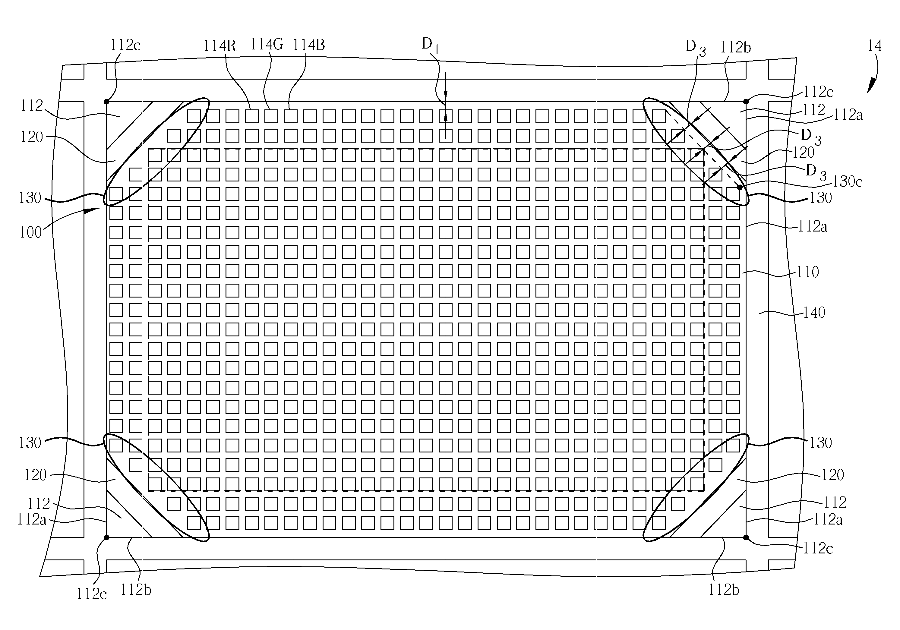
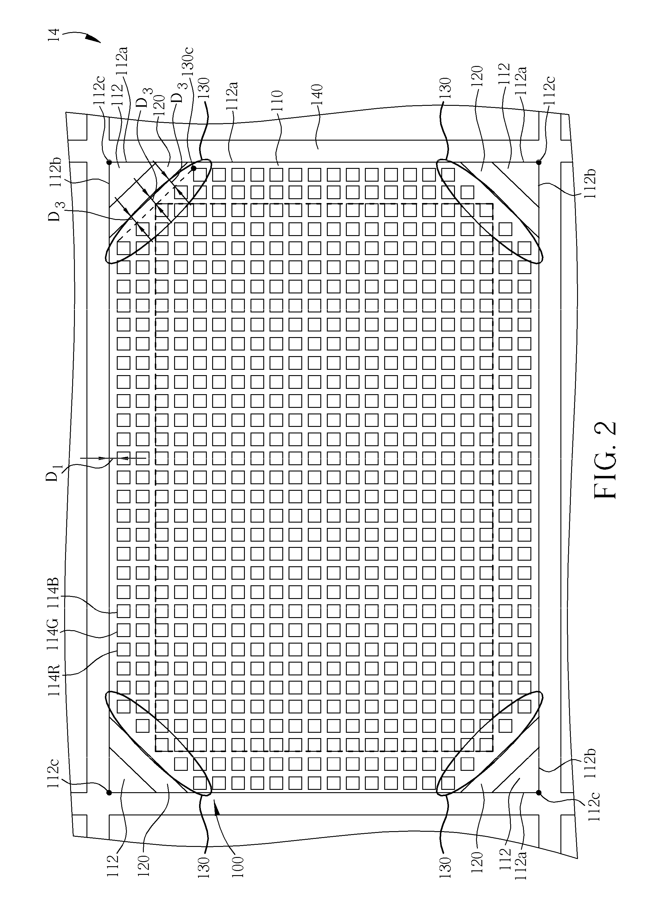
[0019]Please refer to FIGS. 2-4, FIG. 2 is a schematic drawing of a color filter array provided by the first preferred embodiment of the present invention, FIG. 3 is a cross-sectional drawing of the first preferred embodiment, and FIG. 4 is a cross-sectional drawing of a modification of the first preferred embodiment. The first preferred embodiment provides a color filter array 100 having a rectangular die region 110. As shown in FIG. 2, the die region 110 has four die corners 112, each of the die corners 112 is formed by two sides 112a, 112b of the die region 110 while the two sides 112a, 112b are encountered at a corner apex 112c. The color filter array 100 comprises a plurality of color filters 114R, 114G and 114B arranged in a matrix in the die region 110. As shown in FIG. 3, the die region 110 can be defined on a device wafer 102 having a plurality of sub-pixel units 104, and the color filters 114R and 114G, 114B are respectively corresponding to the sub-pixel units 104. Furthe...


PUM


Abstract

A color filter array includes a die region having at least a die corner defined therein, a plurality of color filters arranged in a matrix in the die region, and at least a step-shaped corner positioned corresponding to the die corner.

Description

BACKGROUND OF THE INVENTION [0001]1. Field of the Invention[0002]The present invention relates to a color filter array, and more particularly, to a color filter array capable of obtaining more effective die area.[0003]2. Description of the Prior Art[0004]With the trend toward digital age, the development of display technique and change of broadcasting method that adopts digital signals have made kinds of flat display such as liquid crystal display (LCD), field emission display (FED), organic light emitting diode (OLED), and plasma display panel (PDP) more preferable than conventional cathode ray tube (CRT).[0005]Furthermore, since the micro-display is able to provide larger images than abovementioned displays are by optical method, the micro-display is more preferred on demand for displaying ultra large-sized images. The micro-display possesses another advantage of being easily applied in different displays such as LCD or OLED. For example, the micro-display applied in LCD is so-cal...

Claims


Application Information

Patent Timeline
IPC IPC(8): G02B5/22
CPCG02B5/201G02F1/133351G02F1/133514G02F1/136277G02F2201/56
Inventor WU, YI-TYNG
Owner UNITED MICROELECTRONICS CORP
Why Eureka
Try Eureka