Imaging device, electric charge readout method, and imaging apparatus

a technology of electric charge readout and imaging device, which is applied in the field of imaging device, can solve problems such as sensitivity drop, and achieve the effect of improving pixel characteristics and efficiently operating imaging devices

Inactive Publication Date: 2010-12-23
SONY CORP
View PDF7 Cites 22 Cited by
  • Summary
  • Abstract
  • Description
  • Claims
  • Application Information

AI Technical Summary

Benefits of technology

[0028]Recent miniaturization and other technologies have made it possible to reduce the pixel size to the extent that it approaches the level of the wavelength of light, and the resultant decrease in the amount of light itself incident on (traveling into) a pixel causes improvement in sensitivity characteristics using the existing methods to approach a limit.
[0029]In particular, when the miniaturization advances and the pixel size approaches the level of the wavelength of light, for example, visible light, the ability to collect light decreases even when an OCL or a light collection structure is used.

Problems solved by technology

In this case, the photodiode is incapable of receiving the entire focused light, resulting in decrease in sensitivity.

Method used


Image

  • Imaging device, electric charge readout method, and imaging apparatus
  • Imaging device, electric charge readout method, and imaging apparatus
  • Imaging device, electric charge readout method, and imaging apparatus

Examples


first embodiment

Configuration of Solid-State Imaging Device

[0084]FIG. 5A schematically shows an imaging device 14A according to a first embodiment of the invention.

[0085]FIG. 6 is an enlarged view illustrating part of the pixels illustrated in FIG. 5A.

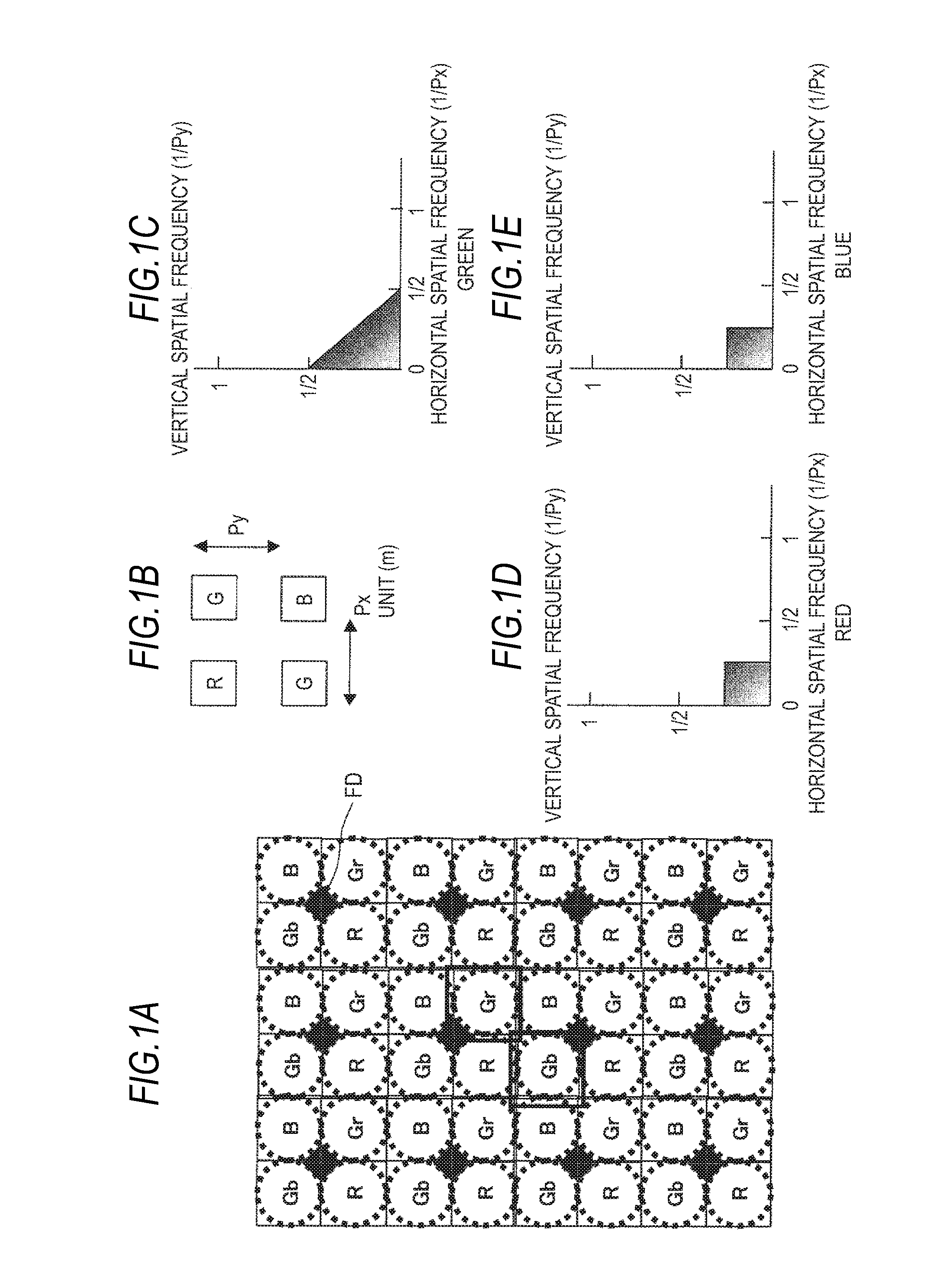
[0086]In FIGS. 5A and 6, the number of in-pixel wiring lines is reduced by an inter-pixel sharing method using vertical and horizontal wiring lines for connecting adjacent pixels, for example, a sharing method using FD (floating diffusion) sections. That is, a floating diffusion (FD) section indicated by a rectangle divided into four is disposed at the center of each set of B, R, Gr, and Gb pixels. The sharing method is an inter-pixel sharing method in which an FD is shared.

[0087]Each open dotted-line circle represents an on-chip lens (OCL) or a light collection structure.

[0088]The rectangles that surround the R, B, Gr, and Gb pixels represent RGB color filters (CFs) in the arrangement based on the Bayer scheme.

[0089]The CFs and the OCLs or light coll...

second embodiment

Configuration of Solid-State Imaging Device

[0111]An imaging device according to a second embodiment of the invention will be described with reference to FIG. 7.

[0112]In FIG. 7, not only are the Gr and Gb pixels configured in the same manner as in the first embodiment but also the B and R pixels are doubled in size in the vertical direction like the G pixels.

[0113]As a result, in the imaging device according to the second embodiment, the above advantageous effect provided by the configuration in the first embodiment is also applied to the B and R pixels. That is, all the pixels can provide the same advantageous effect as that provided in the first embodiment.

[0114]In the second embodiment, all the pixels are doubled in size in the vertical direction. However, since miniaturization makes each single pixel of the imaging device according to the present embodiment fairly small, there is no substantial decrease in resolution resulting from the double-size pixels but the advantageous effe...

third embodiment

Configuration of Solid-State Imaging Device

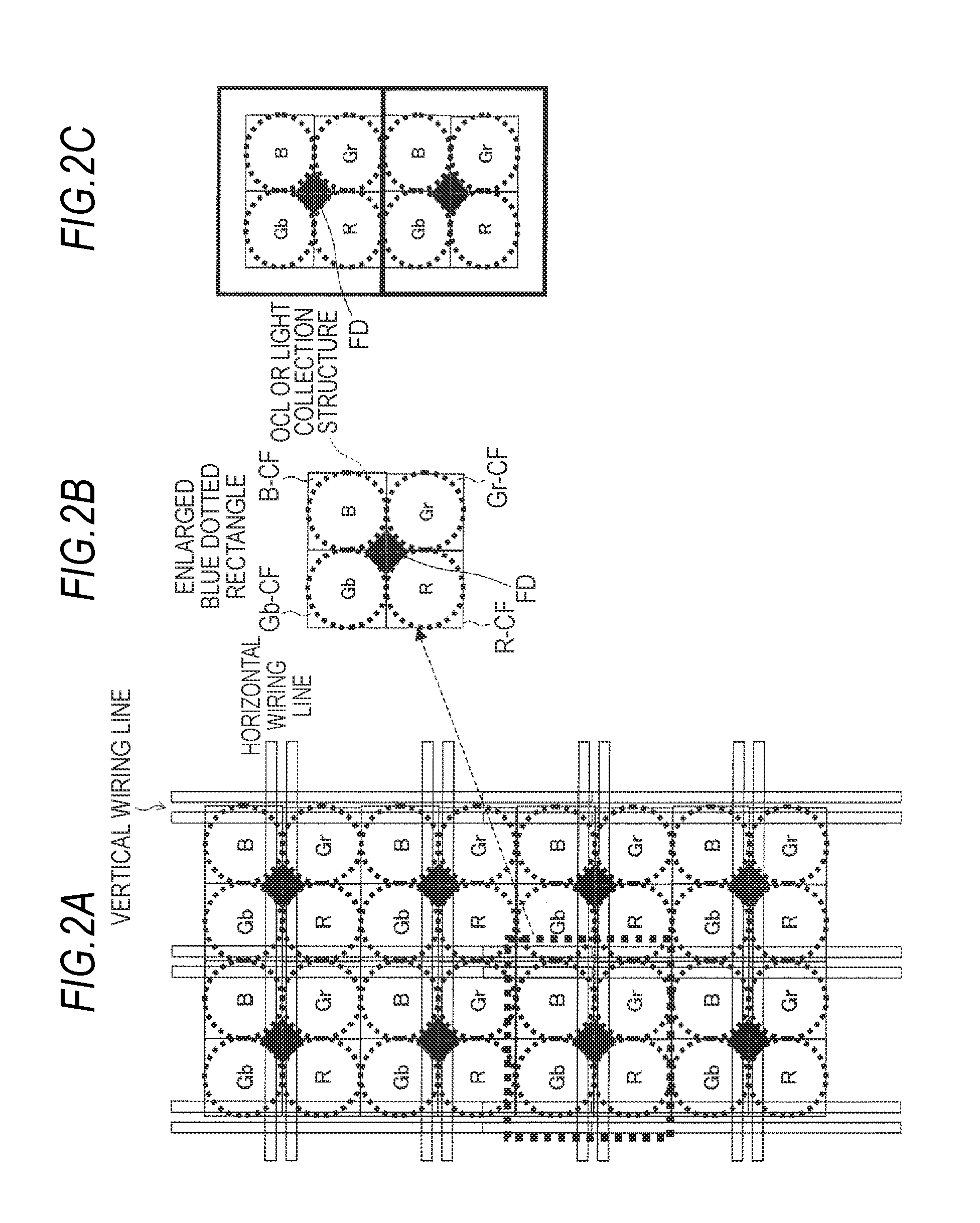
[0116]An imaging device according to a third embodiment of the invention will be described with reference to FIGS. 8A and 8B.

[0117]FIG. 8A shows the arrangement of a plurality of pixels, and FIG. 8B is an enlarged view of part of the arrangement.

[0118]Gr and Gb pixels adjacent to each other in the horizontal direction with a device isolation portion therebetween can be formed by using a single large color filter (CF).

[0119]The third embodiment takes advantage of the flexibility in wiring, which is an advantage of a pixel sharing method and allows use of a structure in which no wiring line passes above the G (Gr and Gb) pixels.

[0120]FIG. 8A illustrates how the wiring lines extend in the vertical and horizontal directions. In this case, since the wiring lines do not block the openings of the Gr and Gb pixels, the area of the opening of each of the Gr and Gb pixels can be maximized.

[0121]Another advantage of the pixel structure illustrated in ...


PUM

PropertyMeasurementUnit
sizeaaaaaaaaaa
sizeaaaaaaaaaa
electric chargeaaaaaaaaaa

Abstract

An imaging device includes: first green pixels; and second green pixels adjacent to the respective first green pixels in a first direction, which is the direction in which electric charge accumulated in the pixels is read, wherein the dimension of the first and second green pixels in a second direction perpendicular to the first direction is twice the dimension of the first and second green pixels in the first direction.

Description

BACKGROUND OF THE INVENTION[0001]1. Field of the Invention[0002]The present invention relates to an imaging device, such as a CMOS image sensor (CIS). The invention particularly relates to an imaging device capable of improving desired pixel characteristics, for example, the sensitivity and the amount of accumulated electric charge (Qs), even when the imaging device is formed of a large number of miniaturized pixels.[0003]2. Description of the Related Art[0004]The invention further relates to a method and an apparatus for reading electric charge from the imaging device.[0005]The invention further relates to a method and an apparatus for performing demosaicing on the imaging device.[0006]The invention further relates to an imaging apparatus including the imaging device described above.[0007]In recent CMOS image sensors and other similar imaging devices, a larger number of pixels are formed in a predetermined region to achieve higher definition images, and miniaturization is underway ...

Claims


Application Information

Patent Timeline
Patent Type & Authority Applications(United States)
IPC IPC(8): G02F1/1335G01R19/00
CPCH01L27/14603H01L27/14621H01L27/14645H04N2209/046H01L27/14689H04N9/045H01L27/14685H01L27/14623H04N25/134
Inventor HA, SANGHOONISHIWATA, HIROAKI
Owner SONY CORP
Why Eureka
Try Eureka