Organic el device and design method thereof

a technology of organic el and device, applied in the direction of semiconductor devices, basic electric elements, electrical apparatus, etc., can solve the problems of low light-extraction efficiency, low light-extraction efficiency of devices, and loss of most emitted light, so as to achieve low drive voltage, no image blur, and high light-extraction efficiency

Inactive Publication Date: 2010-12-30
UDC IRELAND
View PDF7 Cites 15 Cited by
  • Summary
  • Abstract
  • Description
  • Claims
  • Application Information

AI Technical Summary

Benefits of technology

[0013]The present invention aims to provide an organic EL device having high light-extraction efficiency, involving no image blur, and realizing low drive voltage, and to a design method thereof.
[0014]The present inventors conducted extensive studies in order to solve the above-described problems, and have found that a platinum complex compound containing a tetradentate ligand used in the present invention has high electron transportability, that use of this compound as a host material remarkably reduces drive voltage, and that a mixed host, composed of a platinum complex compound containing a tetradentate ligand and a hole transport host material, realizes both high light-emitting efficiency and reduction of the drive potential.
[0030]The present invention can provide an organic EL device involving no image blur, having high light-extraction efficiency, and realizing low drive voltage, and to a design method thereof. These can solve the existing problems pertinent in the art.

Problems solved by technology

For this reason, emitted light tends to be totally reflected on the interfaces, and thus, the light-extraction efficiency is less than 20% and most of the emitted light is lost.
In this case, these devices suffer low light-extraction efficiency, since the totally reflected components (i.e., light entering at an angle higher than the critical angle) cannot be extracted at the interfaces formed between the organic compound layer and the light-extraction surface or the electrode layers.
Thus, the light-extraction efficiency has not been optimized.
In this regard, a combination of a lens and the structure of an organic EL display part has not been optimally designed.
As a result, the light-extraction efficiency is not satisfactory, or image blur occurs when light propagates between the lens and the light-emitting layer.

Method used


Image

  • Organic el device and design method thereof
  • Organic el device and design method thereof
  • Organic el device and design method thereof

Examples


first embodiment

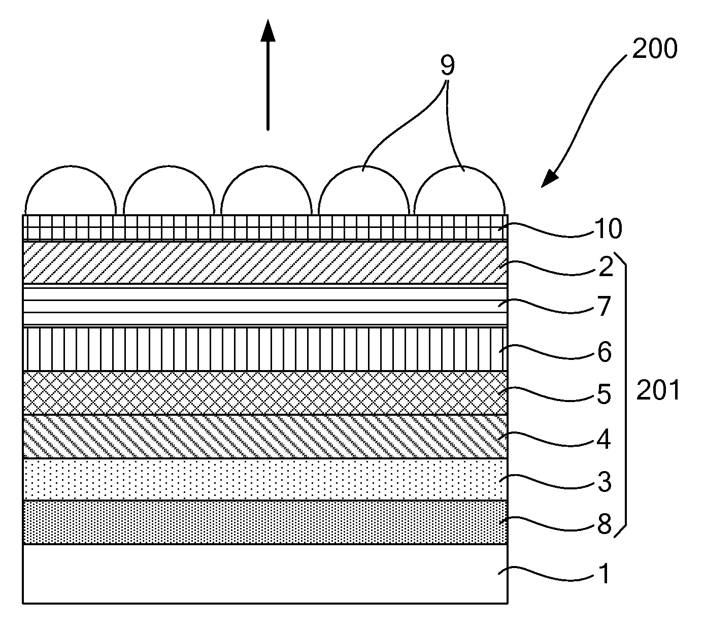
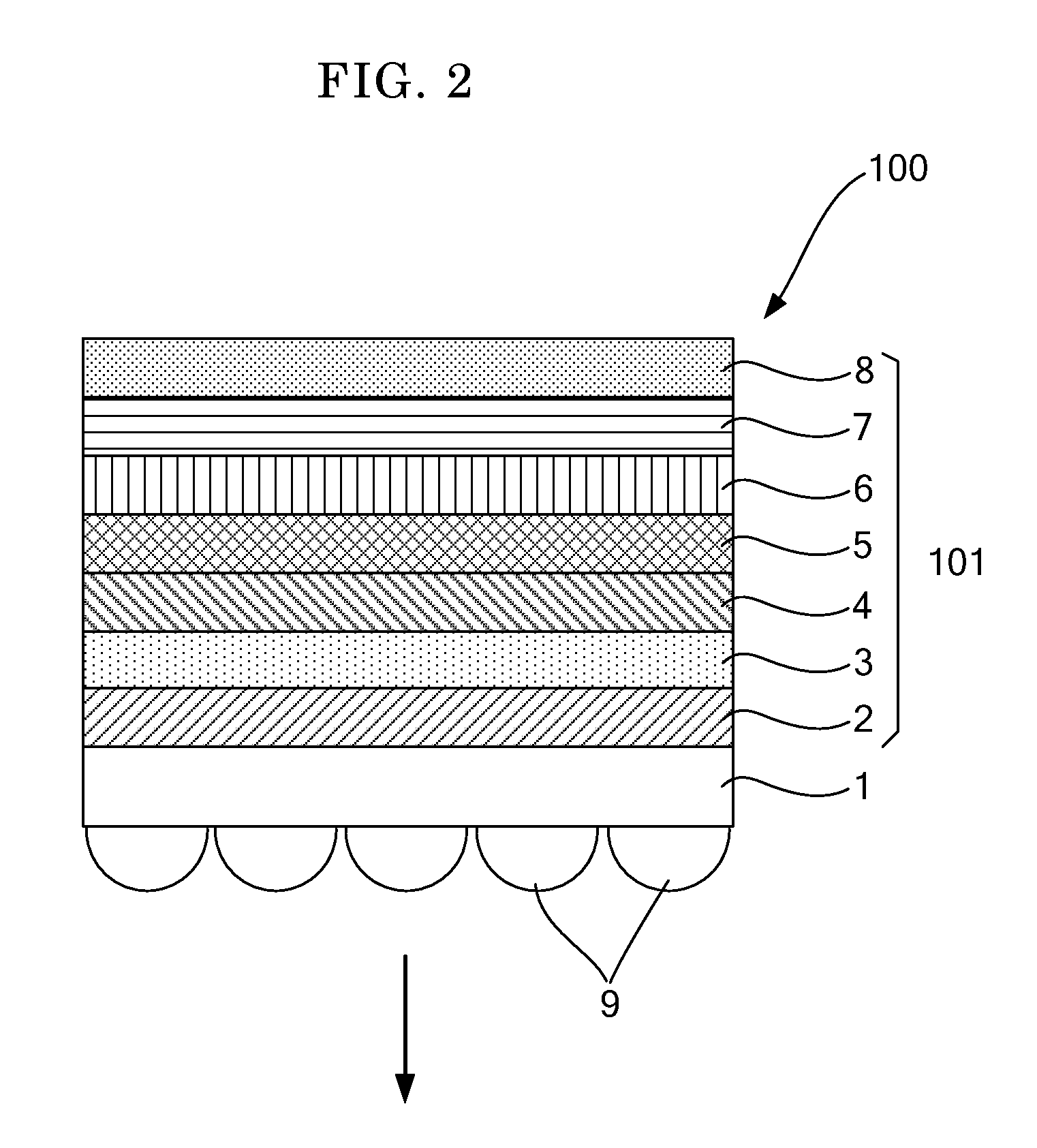
[0089]In a first embodiment, an organic EL display part has a first order microcavity structure whose optical length L(λ) is 1λ, (where λ denotes a wavelength of emitted light). The structure may be of a bottom-emission or top-emission type.

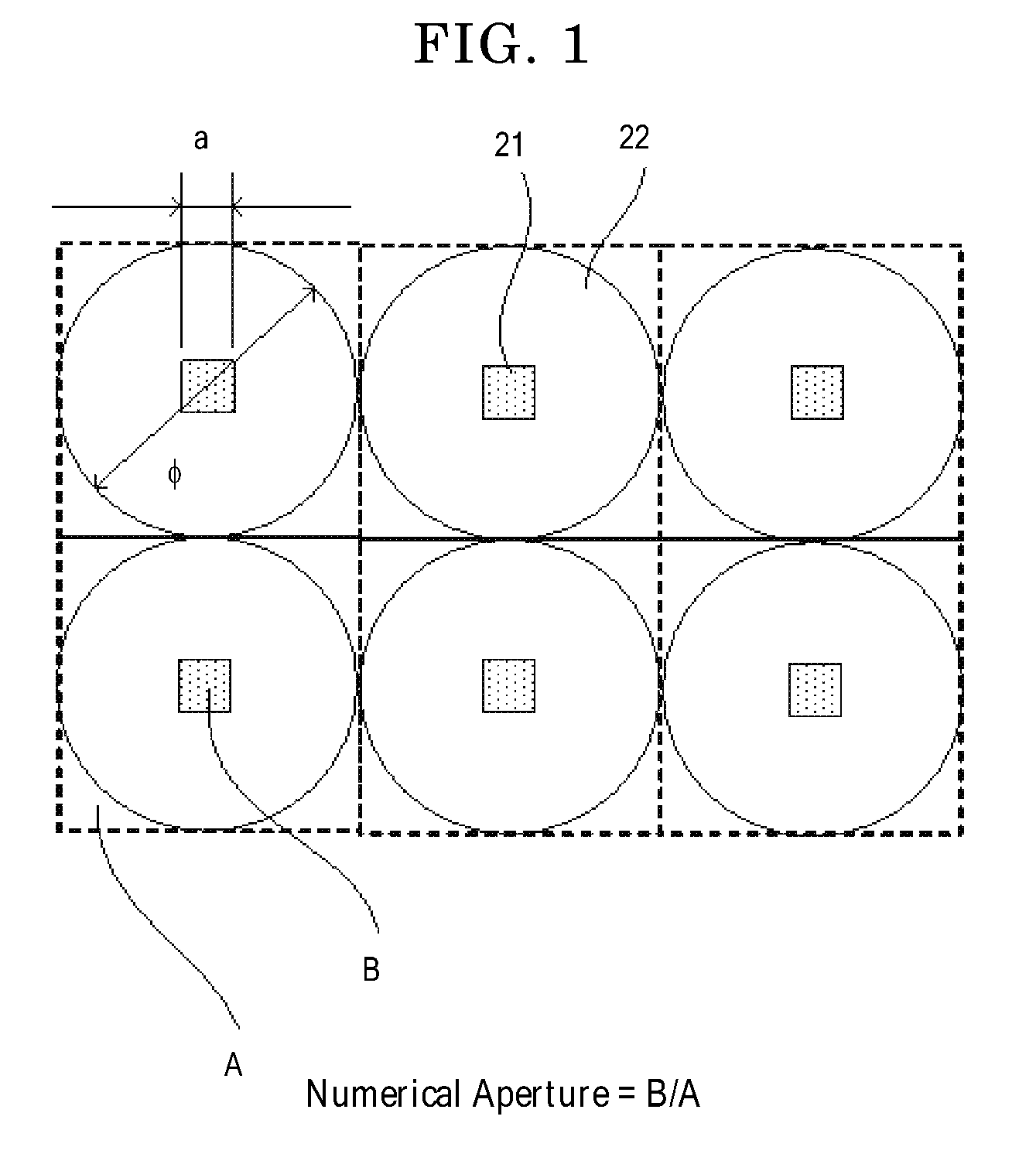
[0090]In this first embodiment, preferably, the ratio of A to B (AM) is greater than 1 and the ratio of φ to a (φ / a) is 1.2 or greater, where A denotes a light-extraction efficiency in terms of front brightness when the lens is placed on the light-extraction surface, B denotes a light-extraction efficiency in terms of front brightness when the lens is not placed on the light-extraction surface, φ denotes an effective diameter of the lens, and a denotes the maximum length of a side of the light-emitting layer. The ratio (φ / a) is more preferably 1.6 or greater, still more preferably 2.5 or greater. The upper limit of the ratio (φ / a) is preferably 4.47.

[0091]Also, preferably, the ratio of C to D (C / D) is greater than 1 and the ratio of φ to a (φ / a) ...

second embodiment

[0092]In a second embodiment, an organic EL display part has a second order microcavity structure whose optical length L(λ) is 2λ, (where λ denotes a wavelength of emitted light). The structure may be of a bottom-emission or top-emission type.

[0093]In this second embodiment, preferably, the ratio of A to B (A / B) is greater than 1 and the ratio of φ to a (φ / a) is 1.4 or greater, where A denotes a light-extraction efficiency in terms of front brightness when the lens is placed on the light-extraction surface, B denotes a light-extraction efficiency in terms of front brightness when the lens is not placed on the light-extraction surface, φ denotes an effective diameter of the lens, and a denotes the maximum length of a side of the light-emitting layer. The ratio (φ / a) is more preferably 1.8 or greater, still more preferably 2.5 or greater. The upper limit of the ratio (φ / a) is preferably 4.47.

[0094]Also, preferably, the ratio of C to D (C / D) is greater than 1 and the ratio of φ to a (φ...

third embodiment

[0095]In a third embodiment, an organic EL display part has a third order microcavity structure whose optical length L(λ) is 3λ (where λ denotes a wavelength of emitted light). The structure may be of a bottom-emission or top-emission type.

[0096]In this third embodiment, preferably, the ratio of A to B (A / B) is greater than 1 and the ratio of φ to a (φ / a) is 1.5 or greater, where A denotes a light-extraction efficiency in terms of front brightness when the lens is placed on the light-extraction surface, B denotes a light-extraction efficiency in terms of front brightness when the lens is not placed on the light-extraction surface, φ denotes an effective diameter of the lens, and a denotes the maximum length of a side of the light-emitting layer. The ratio (φ / a) is more preferably 2.0 or greater, still more preferably 2.5 or greater. The upper limit of the ratio (φ / a) is preferably 4.47.

[0097]Also, preferably, the ratio of C to D (C / D) is greater than 1 and the ratio of φ to a (φ / a) ...


PUM


Abstract

An organic electroluminescence device including an organic electroluminescence display part which includes an anode, a cathode and at least a light-emitting layer disposed therebetween, and a lens which controls an optical path of light emitted from the light-emitting layer, wherein the organic electroluminescence device has a ratio of A to B (A / B) of greater than 1, where A denotes a light-extraction efficiency in terms of front brightness when the lens is placed on a surface from which the light is extracted, and B denotes a light-extraction efficiency in terms of front brightness when the lens is not placed on the surface from which the light is extracted, and wherein the organic electroluminescence device has a ratio of φ to a (φ / a) of 1.0 or greater, where a denotes the maximum length of a side of the light-emitting layer and φ denotes an effective diameter of the lens.

Description

BACKGROUND OF THE INVENTION[0001]1. Field of the Invention[0002]The present invention relates to an organic EL device that exhibits high light-extraction efficiency and reduced image bleeding, and to a design method thereof.[0003]2. Description of the Related Art[0004]Organic electroluminescence devices (organic EL devices) are self-emitting-type display devices, and are used in displays and lightings. Organic EL displays have several advantages over conventional CRTs or LCDs in terms of display performances, such as high visibility and no viewing-angle-dependency. Furthermore, organic EL lightings have advantages in that they can be made to be lightweight and thin-layered. In addition, organic EL lightings may open up a possibility of lightings with novel shapes through use of flexible substrates.[0005]Although such organic EL devices possess several excellent characteristics, the refractive indices of the constituent layers thereof, including a light-emitting layer, are generally ...

Claims


Application Information

Patent Timeline
Patent Type & Authority Applications(United States)
IPC IPC(8): H01L51/52
CPCH01L51/5275H01L51/5265H10K50/852H10K50/858
Inventor SONODA, SHINICHIROTAKABASHI, TOSHIROTOBISE, MANABU
Owner UDC IRELAND
Why Eureka
Try Eureka