

Joining structure and a substrate-joining method using the same
- Summary
- Abstract
- Description
- Claims
- Application Information
AI Technical Summary
Benefits of technology
Problems solved by technology
Method used
Image

Examples
Embodiment Construction
[0013]Hereinafter, embodiments of the present invention will be described in detail with reference to the accompanying drawings. However, the present invention is not limited to the following embodiments.
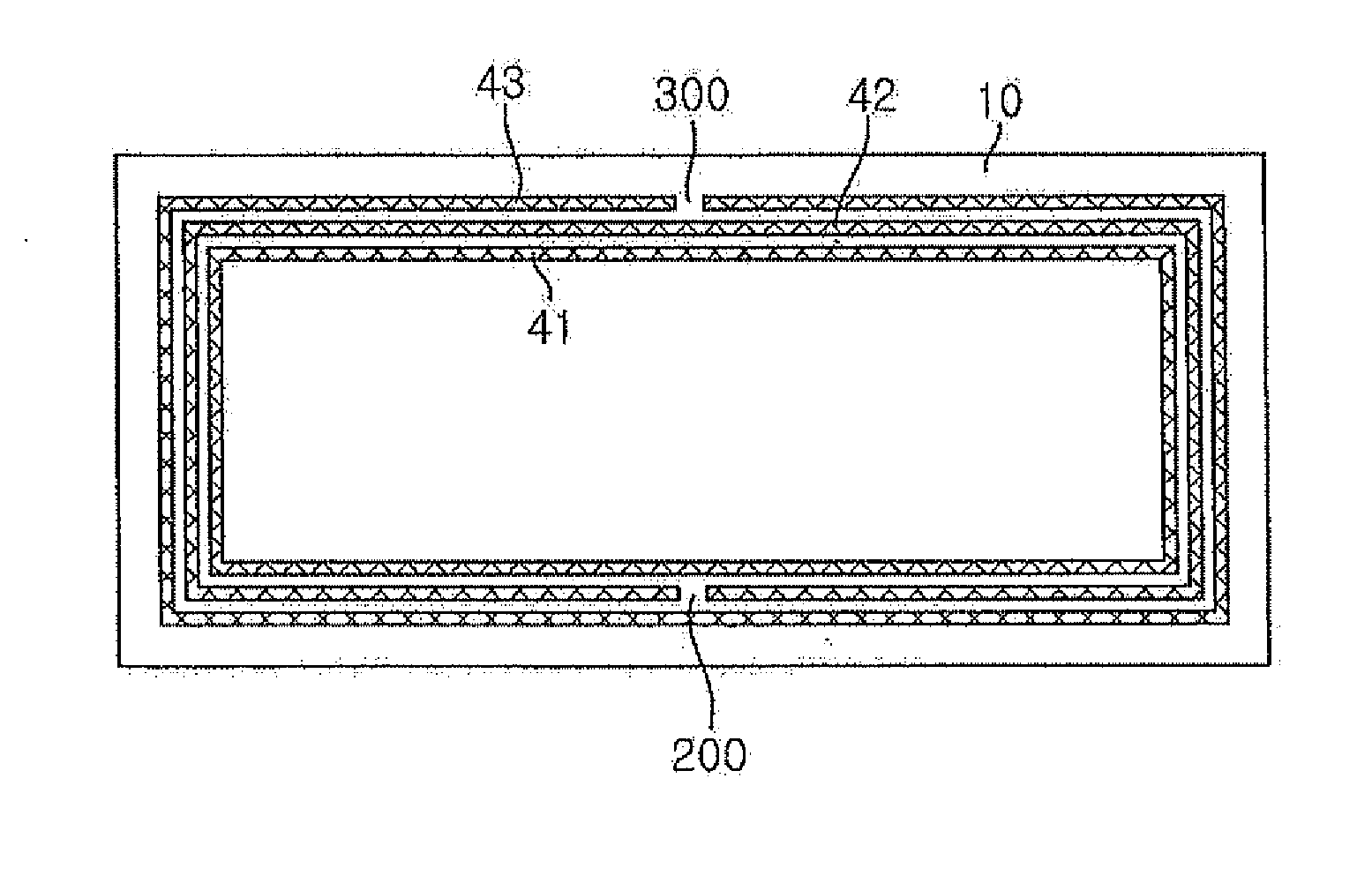
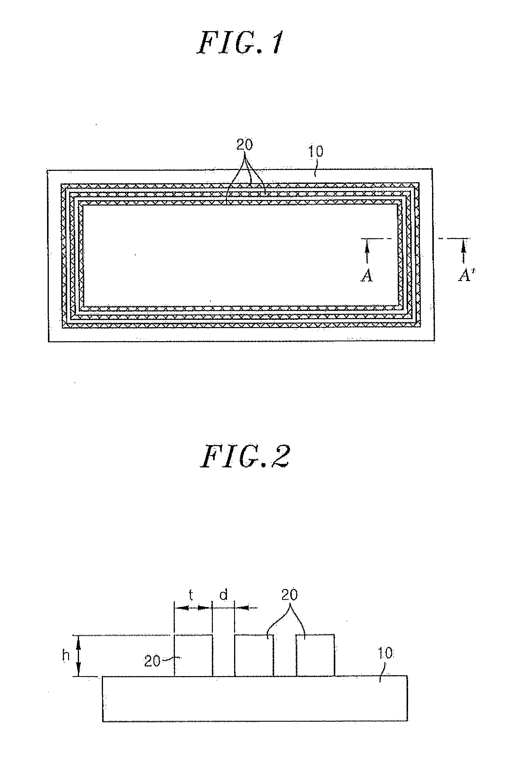
[0014]FIG. 1 is a top plan view of a bonding structure in accordance with an embodiment of the present invention, and FIG. 2 is a cross-sectional view taken along line A-A′ in FIG. 1.
[0015]Referring to FIGS. 1 and 2, the bonding structure includes a substrate 10 and multiple bonding patterns 20. The substrate 10 may be formed of glass, silicon, or other appropriate material. Further, a circuit or device, a mechanical structure and the like may be formed on the substrate 10.
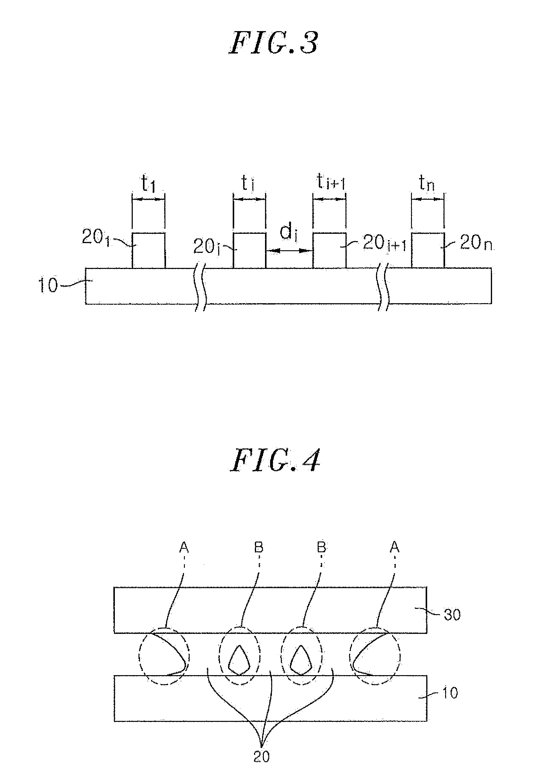
[0016]The multiple bonding patterns 20 are provided on the substrate 10. The bonding patterns 20 are provided for bonding the substrate 10 to another structure, and may be formed of a material which is capable of bonding. The bonding patterns 20 may include one or several layers. In an embodiment of the present in...
PUM
 Abstract
Description
Claims
Application Information