

Flexible piezoelectric device and flexible capacitor manufactured by the same, and manufacturing method for flexible sensors
a manufacturing method and piezoelectric technology, applied in the direction of electrical transducers, transducer types, electric/electrostrictive transducers, etc., can solve the problems of difficult commercialization, high cost of using expensive single-crystal silicon substrates, and material electrical properties not having superior electrical properties, etc., to achieve stable rectifying the generated current, saving the cost of using expensive single-crystal silicon substrates, and preventing damage to silicon substrates
- Summary
- Abstract
- Description
- Claims
- Application Information
AI Technical Summary
Benefits of technology
Problems solved by technology
Method used
Image

Examples
Embodiment Construction
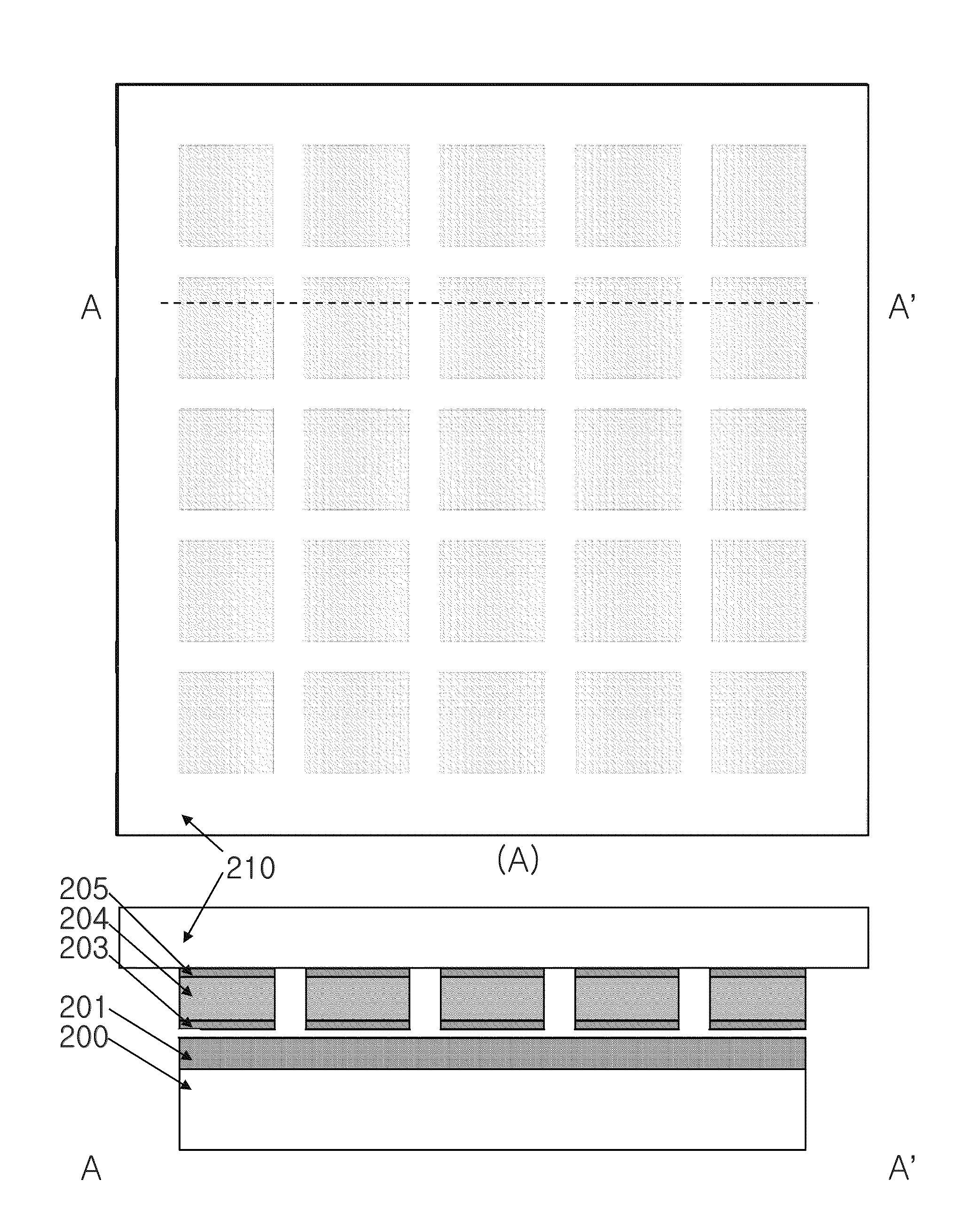
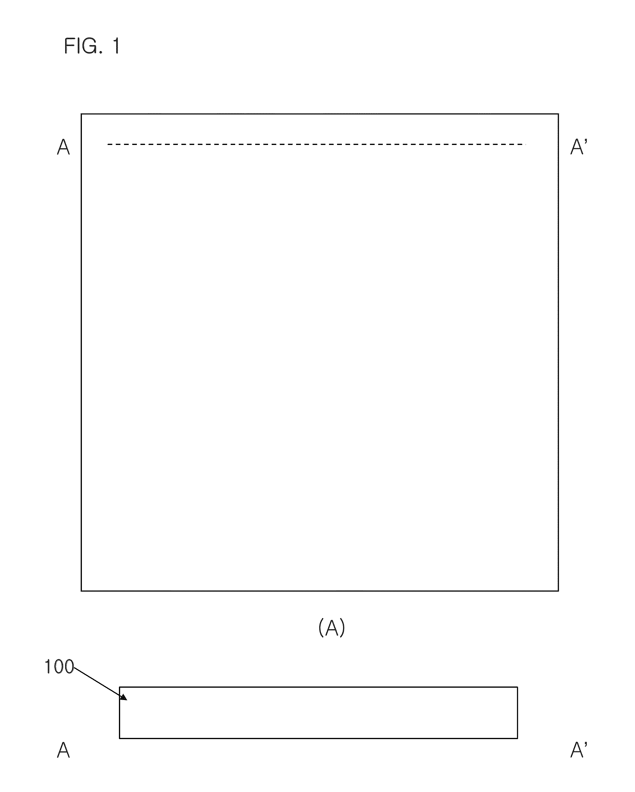
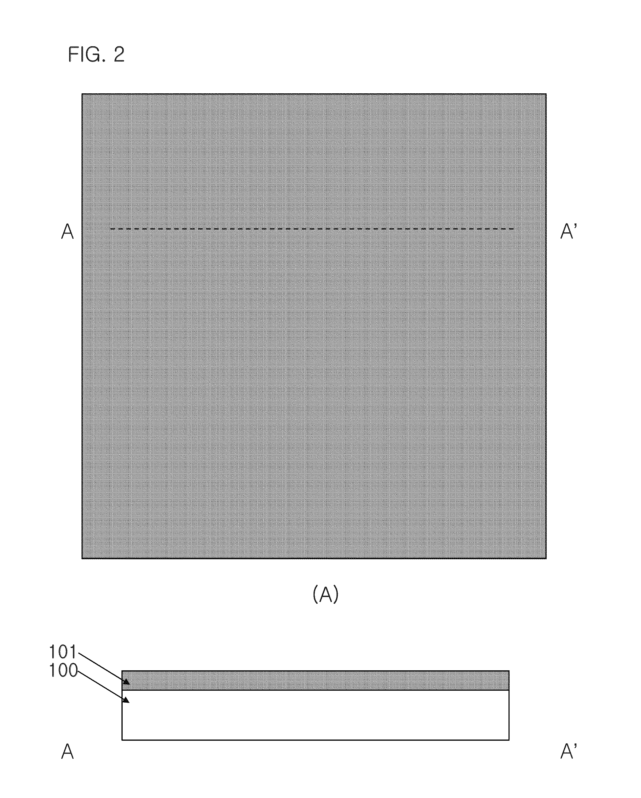
[0031]The advantages, features and aspects of the invention will become apparent from the following description of the embodiments with reference to the accompanying drawings, which is set forth hereinafter. The following embodiments are provided to convey the spirit of the present invention to those skilled in the art. Accordingly, the present invention is not limited to the following embodiments but may be embodied in other forms. In the attached drawings, width, length, thickness, etc. may be exaggerated for convenience of illustration. In the drawings, like reference numerals denote like elements. And, all the attached drawings are plan views or partial cross-sectional views (along line A-A′, B-B′ or C-C′).
[0032]According to the present invention, a device to be transferred to a flexible substrate (i.e., a substrate that can bend unlike the hard substrate, for example, a plastic substrate) is prepared on a metal oxide layer on a silicon substrate, and the metal oxide is selectiv...
PUM
| Property | Measurement | Unit |
|---|---|---|
| Temperature | aaaaa | aaaaa |
| Temperature | aaaaa | aaaaa |
| Flexibility | aaaaa | aaaaa |
Abstract
Description
Claims
Application Information