Color filter substrate and liquid crystal display device

a color filter substrate and liquid crystal display technology, applied in the direction of optics, instruments, optical elements, etc., can solve the problems of difficult color design of such a liquid crystal display panel, difficulty in alignment control by rubbing alignment films, and disclination of surrounding normal dots, so as to suppress the occurrence of both a switching domain and disclination, and suppress the effect of a decrease in the aperture ratio

Inactive Publication Date: 2011-01-06
SHARP KK
View PDF9 Cites 14 Cited by
  • Summary
  • Abstract
  • Description
  • Claims
  • Application Information

AI Technical Summary

Benefits of technology

[0035]The color filter substrate and the liquid crystal display device of the present invention enable easy color design for a liquid crystal display panel, can suppress occurrence of both a switching domain and disclination, and can also suppress a decrease in the aperture ratio.
[0036]The present invention is described in more detail based on the following embodiments with reference to the drawings. The present invention is not limited to these embodiments.
[0037]The liquid crystal display device of the present embodiment is a TN liquid crystal display device provided with a TFT substrate and a color filter substrate which face each other. The liquid crystal display device has spacers to maintain a certain space between the substrates. The TFT substrate and the color filter substrate are attached via a sealing agent. A liquid crystal material containing liquid crystal molecules (nematic liquid crystals) having positive dielectric anisotropy is filled between the substrates such that a liquid crystal layer is formed. The liquid crystal layer is in a horizontal alignment mode in which liquid crystal molecules are aligned substantially in parallel with the substrates when no voltage is applied between the substrates. Here, the TFT substrate has a common structure. For example, the TFT substrate has, on a transparent substrate, wirings such as source lines, gate lines, and Cs lines (storage capacitor wirings); TFTs which are switching elements; an insulating layer; pixel electrodes formed of a transparent conductive film; and a rubbed alignment film.
[0038]FIG. 1 are schematic views each illustrating a color filter substrate of Embodiment 1 according to the present invention: FIG. 1(a) shows a plan view of the substrate; and FIG. 1(b) shows a cross-sectional view taken along the A1-B1 line in FIG. 1(a). The color filter substrate 1 of the present embodiment has a structure in which the following components are stacked on one main face (on the liquid crystal layer side) of a transparent substrate 10, in the order of: a black matrix 20 serving as a light-shielding member to shield from light a portion between adjacent dots; a filter layer 30 having red (R) color filters 31R, green (G) color filters 31G, and blue (B) color filters 31B are arranged therein in a manner that a filter is provided for a dot; a counter electrode (not illustrated) formed of a transparent conductive film; and a rubbed alignment film (not illustrated)
[0039]The black matrix 20 has portions (source light-shielding portions) 21 which are formed along the source lines of the TFT substrate (counter substrate) and extend in the vertical direction in FIG. 1; thick portions (gate light-shielding portions) 22 which are formed along the gate lines of the TFT substrate and extend in the horizontal direction in FIG. 1; and thin portions (Cs light-shielding portions) 23 which are formed along the Cs lines of the TFT substrate and extend in the horizontal direction in FIG. 1. The gate light-shielding portions 22 and the Cs light-shielding portions 23 are arranged parallel to each other, and the source light-shielding portions 21 perpendicularly intersect the gate light-shielding portions 22 and the Cs light-shielding portions 23. Each opening region surrounded by the source light-shielding portions 21 and the gate light-shielding portions 22 is generally one dot (a single-color region constituting a pixel, i.e., a sub pixel). In this way, each dot is surrounded by the source light-shielding portions 21 and the gate light-shielding portions 22 of the black matrix 20. The color filter substrate 1 employs a stripe arrangement in which the dots of R, G, and B are arranged in stripes. The three dots of R, G, and B, which are adjacent to each other in the horizontal direction in FIG. 1, constitute one pixel (the smallest unit of a display image) in the liquid crystal display device of the present embodiment. The TFT substrate has for each dot a TFT as a switching element, and a pixel electrode connected to the TFT.
[0040]The color filters 31R, the color filters 31G, and the color filters 31B are basically arranged such that a color filter corresponds to the opening of a dot (dot opening), and color filters arranged adjacent to each other in the vertical and horizontal directions in FIG. 1 have a space therebetween. Each of the color filter 31R, the color filter 31G, and the color filter 31B has regions (dot portions) constituting respective dots which are of the same color (same-color dots) in the vertical direction in FIG. 1, and those dot portions are partially connected to each other on the black matrix 20. Specifically, the color filters 31R, the color filters 31G, and the color filters 31B respectively have connecting portions 32R, connecting portions 32G, and connecting portions 32B, and each connecting portion has a substantially rectangular shape in a plan view and partially connects dot portions for adjacent same-color dots at apart of the border of same-color dots. That is, each color filter in a plan view has a shape with narrow portions at the connecting portions 32R, the connecting portions 32G, and the connecting portions 32B.

Problems solved by technology

Further, disclination in a part of dots tends to cause disclination in the surrounding normal dots.
Further, color design for such a liquid crystal display panel is difficult because the chromaticity changes at the overlapping portion.
As a result, the inventors have found the cause of disclination.
These elevation changes have been found to be the cause of disclination in a liquid crystal display device provided with the conventional color filter substrate 101.
In addition, alignment control by rubbing of alignment films may become difficult near a portion with a steep elevation change.

Method used


Image

  • Color filter substrate and liquid crystal display device
  • Color filter substrate and liquid crystal display device
  • Color filter substrate and liquid crystal display device

Examples


embodiment 1

[0037]The liquid crystal display device of the present embodiment is a TN liquid crystal display device provided with a TFT substrate and a color filter substrate which face each other. The liquid crystal display device has spacers to maintain a certain space between the substrates. The TFT substrate and the color filter substrate are attached via a sealing agent. A liquid crystal material containing liquid crystal molecules (nematic liquid crystals) having positive dielectric anisotropy is filled between the substrates such that a liquid crystal layer is formed. The liquid crystal layer is in a horizontal alignment mode in which liquid crystal molecules are aligned substantially in parallel with the substrates when no voltage is applied between the substrates. Here, the TFT substrate has a common structure. For example, the TFT substrate has, on a transparent substrate, wirings such as source lines, gate lines, and Cs lines (storage capacitor wirings); TFTs which are switching elem...

example 1

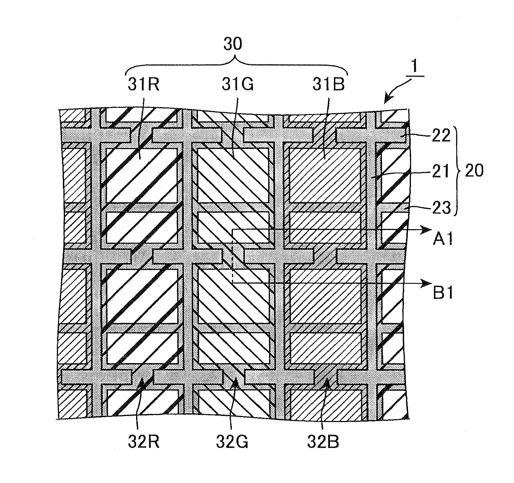
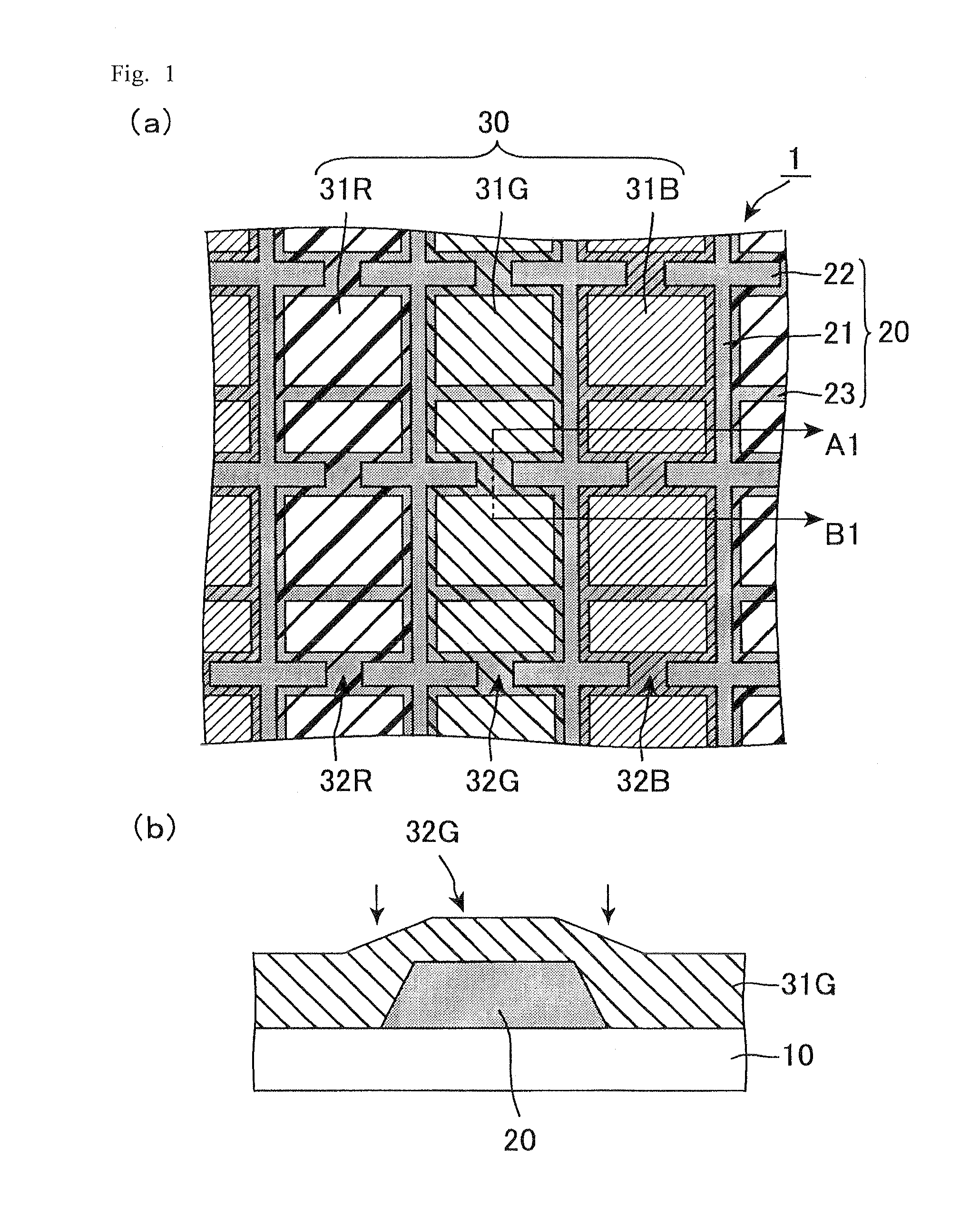
[0090]As illustrated in FIG. 7, a color filter substrate that is the same as the color filter substrate 1 illustrated in FIG. 1 was produced. Specifically, a black photosensitive resin composition was applied on a glass substrate and was patterned into the black matrix 20 having a thickness of 1.1 μm. On the black matrix 20, liquid color resists were applied and patterned into the respective color filters 31R, color filters 31G, and color filters 31B, in the stated order. The color filter 31R, the color filter 31G, and the color filter 31B each had a thickness of 1.9 μm in the dot openings, and had a thickness of from 1.0 to 1.4 μm on the black matrix 20. As a result, the color filter 31R, the color filter 31G, and the color filter 31B had elevation changes, resulting from the black matrix 20, of from 0.2 to 0.6 micrometers.

[0091]The dot pitch in the vertical direction (vertical pitch) in FIG. 7 was 159 μm. The dot pitch in the horizontal direction (horizontal pitch) in FIG. 7 was 5...

example 2

[0093]Liquid crystal display devices for the verification test were produced which had the same configuration as that of the liquid crystal display device of Example 1, except that the ratio We / Wb was changed to 0.38.


PUM

PropertyMeasurementUnit
widthaaaaaaaaaa
widthaaaaaaaaaa
thicknessaaaaaaaaaa

Abstract

The present invention provides a color filter substrate and a liquid crystal display device which enable easy color design for a liquid crystal display panel, can suppress both a switching domain and disclination, and can also suppress a decrease in the aperture ratio. The color filter substrate of the present invention has a structure in which adjacent color filters have respective projections that project toward each other and are in contact with each other on a light-shielding member; a structure in which color filter regions for same-color dots adjacent to each other are partially connected on the shielding member; or a structure in which the above structures are combined.

Description

TECHNICAL FIELD[0001]The present invention relates to a color filter substrate and a liquid crystal display device. More specifically, the present invention relates to a color filter substrate having a rubbed alignment film, and to a liquid crystal display device having the color filter substrate.BACKGROUND ART[0002]Liquid crystal display devices are widely used for electronic equipment such as monitors, projectors, cellular phones, and PDAs (Personal Digital Assistants) because of their advantages such as the slim profile, light weight, and low power consumption. Especially TFT-type liquid crystal display devices (hereinafter also referred to as “TFT-LCDs”) are widely used and the market for TFT-LCDs is expected to be further expanded. This situation brings a demand for further improvement of image qualities of TFT-LCDs.[0003]FIG. 8 is a conceptual diagram illustrating the rubbing directions for alignment films and the twisting direction of liquid crystals, in a plan view of a dot ...

Claims


Application Information

Patent Timeline
Patent Type & Authority Applications(United States)
IPC IPC(8): G02F1/1335
CPCG02B5/201G02B5/223G02F2001/13373G02F1/133707G02F1/133514G02F1/13373
Inventor SHIRAI, TOHRUAKITOMO, MASAHARUMORINAGA, JUNICHI
Owner SHARP KK
Why Eureka
Try Eureka