Liquid crystal display device

a liquid crystal display and display device technology, applied in non-linear optics, instruments, optics, etc., can solve the problems of increasing manufacturing costs, increasing man-hours, and increasing manufacturing throughput, so as to prevent the generation of air bubbles in the display region and improve the reliability of the seal portion

Active Publication Date: 2011-01-13
JAPAN DISPLAY INC +1
View PDF6 Cites 36 Cited by
  • Summary
  • Abstract
  • Description
  • Claims
  • Application Information

AI Technical Summary

Benefits of technology

[0033]According to an aspect of the invention, the difference between the gap between the TFT substrate and the counter substrate in the display region and the gap between the TFT substrate and the counter substrate in the seal portion can be eliminated or can be always maintained at a fixed value. Accordingly, in a liquid crystal display device of a type which injects liquid crystal by a one drop fill method, the reliability of the seal portion can be improved. Moreover, the generation of air bubbles in the display region can be prevented.

Problems solved by technology

However, when the gap between the TFT substrate and the counter substrate is small, and the display area of the liquid crystal display device is large, the injection requires a great deal of time, which lengthens manufacturing throughput and thus increases the manufacturing cost.
However, a number of man-hours are required for sealing liquid crystal into the individual liquid crystal cells.
In this case, when the amount of liquid crystal to be dropped is too small, air bubbles are generated in the liquid crystal cell 1, and when the amount of liquid crystal to be dropped is too large, liquid crystal enters between the sealing material 20 and the TFT substrate or between the sealing material 20 and the counter substrate, causing sealing defects.

Method used


Image

  • Liquid crystal display device
  • Liquid crystal display device
  • Liquid crystal display device

Examples


first embodiment

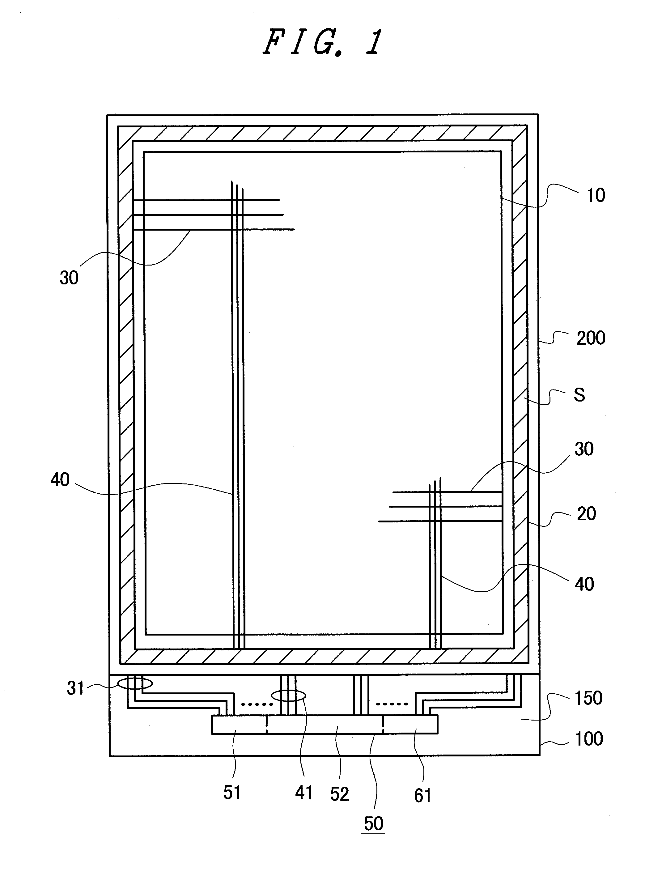
[0054]FIG. 1 is a plan view of a small liquid crystal display device used for mobile phones or the like as an example of a product to which the invention is applied. In FIG. 1, a counter substrate 200 is disposed above a TFT substrate 100. A liquid crystal layer is interposed between the TFT substrate and the counter substrate. The TFT substrate and the counter substrate are bonded together with a sealing material 20 formed in a frame portion. In FIG. 1, since liquid crystal is sealed by a one drop fill method, a filling port is not formed.

[0055]The TFT substrate 100 is formed larger than the counter substrate 200. In a portion of the TFT substrate 100 extended from the counter substrate 200, a terminal portion 150 for supplying a power supply, video signals, scanning signals, and the like to a liquid crystal cell 1 is formed.

[0056]In the terminal portion 150, an IC driver 50 for driving scanning lines, video signal lines, and the like is disposed. The IC driver 50 is divided into t...

second embodiment

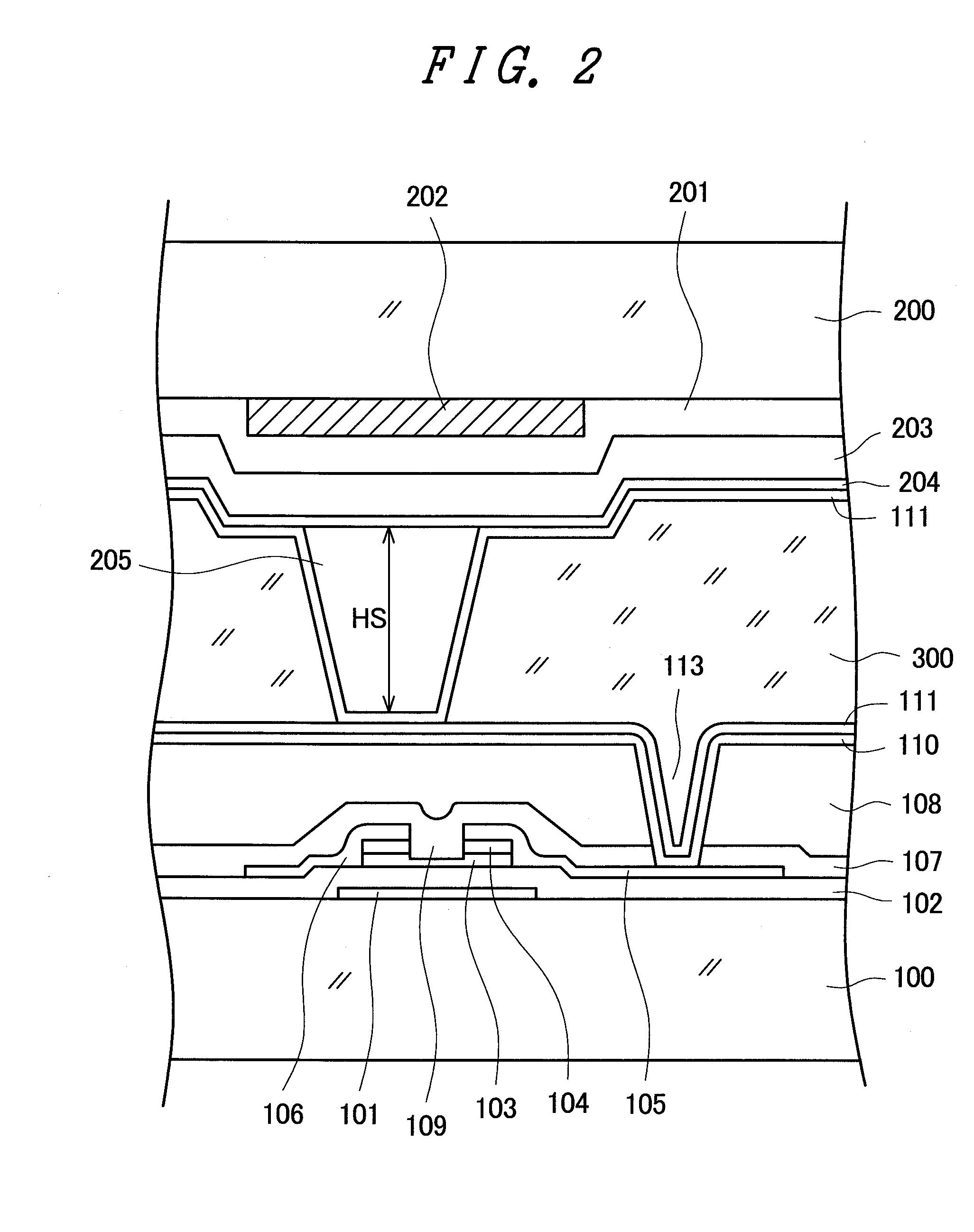
[0091]FIG. 9 is a cross-sectional view of a seal portion according to a second embodiment of the invention. The configuration of a display region in the embodiment is the same as that of the first embodiment. In FIG. 9, the gap between the TFT substrate 100 and the counter substrate 200 in the seal portion is determined by the columnar spacer 205 in the same manner as the first embodiment.

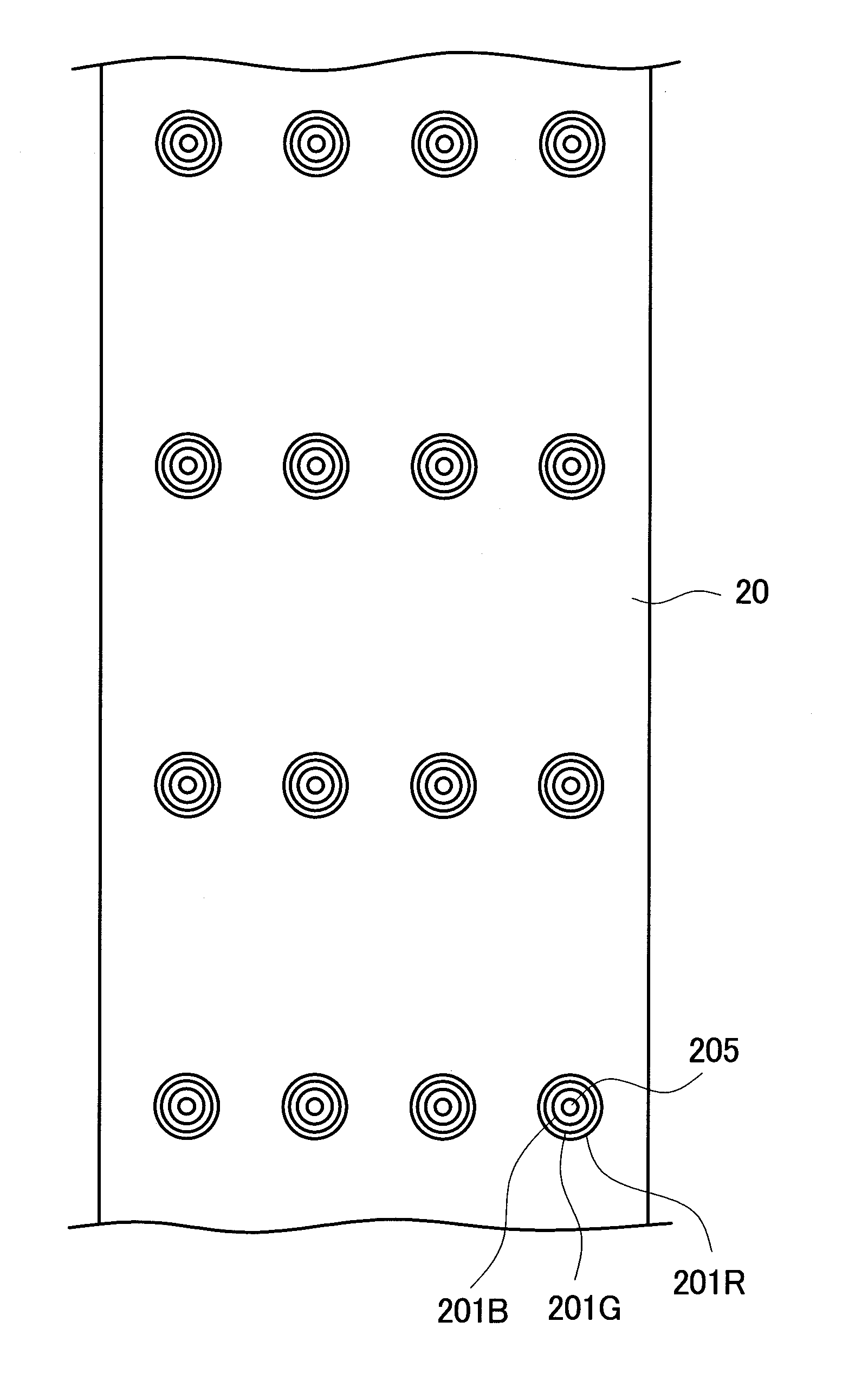
[0092]In the embodiment, the red color filter 201R, the green color filter 201G, and the blue color filter 201B are stacked and formed in an island shape below the columnar spacer 205 in the seal portion. Since each of the color filters 201R, 201G, and 201B is formed in an island shape, the thickness thereof is likely to be smaller than that of the color filter 201 formed in a stripe in the display region. Also the overcoat film 203 formed on the color filter becomes thin when it is formed on the island-shaped color filter due to the leveling effect.

[0093]As described above in the embodiment, the g...

third embodiment

[0098]FIG. 12 is a plan view of a seal portion according to a third embodiment of the invention. The configuration of FIG. 12 is different from that of the first embodiment or the second embodiment in that a weir 500 for stopping the alignment film 111 is disposed substantially at the central portion of the seal portion. The weir 500 is formed along the entire sealing material 20.

[0099]The presence of the alignment film 111 between the sealing material and the substrate impairs the adhesive properties between the sealing material and the substrate. The alignment film 111 is applied in the display region in the form of liquid by an inkjet method or the like and thereafter solidified by baking. Upon applying the alignment film 111 in the form of liquid, when the alignment film 111 flows into the seal portion, the reliability of the seal portion is reduced.

[0100]In the embodiment, for preventing the alignment film 111 in the form of liquid from entering the entire seal portion even if ...


PUM

PropertyMeasurementUnit
thickaaaaaaaaaa
thicknessaaaaaaaaaa
thicknessaaaaaaaaaa

Abstract

In a liquid crystal display device in which liquid crystal is sealed by a one drop fill method, the gap between a TFT substrate and a counter substrate is defined by a columnar spacer in a display region, and the gap between them is defined by a columnar spacer also in a seal portion. In the display region, one layer of a color filter is formed below the columnar spacer. In the seal portion, two layers of island-shaped color filters are formed. With this configuration, the gap between the TFT substrate and the counter substrate can be maintained equal between the display region and the seal portion. Even when the process for forming the columnar spacer varies, it is possible to eliminate a change in difference between the gap between the TFT substrate and the counter substrate in the display region and the gap in the seal portion.

Description

CLAIM OF PRIORITY[0001]The present application claims priority from Japanese application serial No. 2009-161610 filed on Jul. 8, 2009, the content of which is hereby incorporated by reference into this application.BACKGROUND OF THE INVENTION[0002]1. Field of the Invention[0003]The present invention relates to a liquid crystal display device and more particularly to a liquid crystal display device which does not cause air bubbles or liquid crystal leakage and thus is improved in reliability in a configuration of filling liquid crystal between a TFT substrate and a counter substrate by a one drop fill method.[0004]2. Description of the Related Art[0005]In liquid crystal display devices, liquid crystal is filled between a TFT substrate on which pixels each having a pixel electrode and a thin film transistor (TFT) are formed in a matrix and a counter substrate on which color filters and the like are formed, and an image is formed by controlling the molecules of the liquid crystal by an ...

Claims


Application Information

Patent Timeline
Patent Type & Authority Applications(United States)
IPC IPC(8): G02F1/1335G02F1/1339
CPCG02F1/133514G02F1/13394G02F1/13452G02F1/136286G02F1/13396G02F1/133388G02F1/1337G02F1/1339
Inventor YAMAMOTO, TAKASHISUGANO, TOMOYAKAMADA, TAKAMITSU
Owner JAPAN DISPLAY INC
Why Eureka
Try Eureka