Semiconductor storage device and refresh control method thereof
Inactive Publication Date: 2011-01-13
NEC ELECTRONICS CORP
View PDF12 Cites 13 Cited by
Summary
Abstract
Description
Claims
Application Information
AI Technical Summary
This helps you quickly interpret patents by identifying the three key elements:
Problems solved by technology
Method used
Benefits of technology
Benefits of technology
[0046]In the pseudo SRAM whose capacity is made large by employing a configuration with many banks, to simultaneous activate on a basis of a method as a conventional SRAM, it is required to simultaneously activating many adjacent banks. Therefore, the peak current increases so that the load on the current capacity of an internal power source system circuit and the GND increases. Moreover, caused by the neighboring arrangement of the layout, mutual interferences, such as a drop in an internal power source and floating of a GND connected to the memory cell array. For this reason, in a sense amplifier connected to the memory cell array, the supply of the level sufficient for the driving signal is prevented. As a result, the activating operation is delayed, and the potential of a Digit (bit line) pair is prevented from being made wide within the activation time of the word. Also, the holding level of the memory cell data is decreased, which results in a problem that the data hold time of the memory cell is lacked and the data in the memory cell is broken.
[0050]In a configuration of the present invention, in a semiconductor storage device whose capacity is made large by employing the many-bank configuration, the refresh operation is performed on a group of bank which are not adjacent to one another, in accordance with the combination of the bank simultaneous activation (the combination of banks being simultaneously activated) and the activating order. Thus, the interference of the adjacent banks can be avoided while the peak current in one refresh operation is decreased over the conventional technique. Further, the lack of the data hold time of the memory cell is solved, so that the data break in the memory cell that is caused by the lack of the data hold time can be prevented.
Problems solved by technology
If a conventional pseudo SRAM constructed by a plurality of banks is applied in a case of a pseudo SRAM having a large memory capacity, there is a problem that a lack of data hold time of the memory cell causes the memory cell data to be broken.
Moreover, caused by the neighboring arrangement of the layout, mutual interferences, such as a drop in an internal power source and floating of a GND connected to the memory cell array.
Also, the holding level of the memory cell data is decreased, which results in a problem that the data hold time of the memory cell is lacked and the data in the memory cell is broken.
Method used
Image
Click on the blue label to locate the original text in one second.
Reading with bidirectional positioning of images and text.
Examples
first embodiment
Configuration
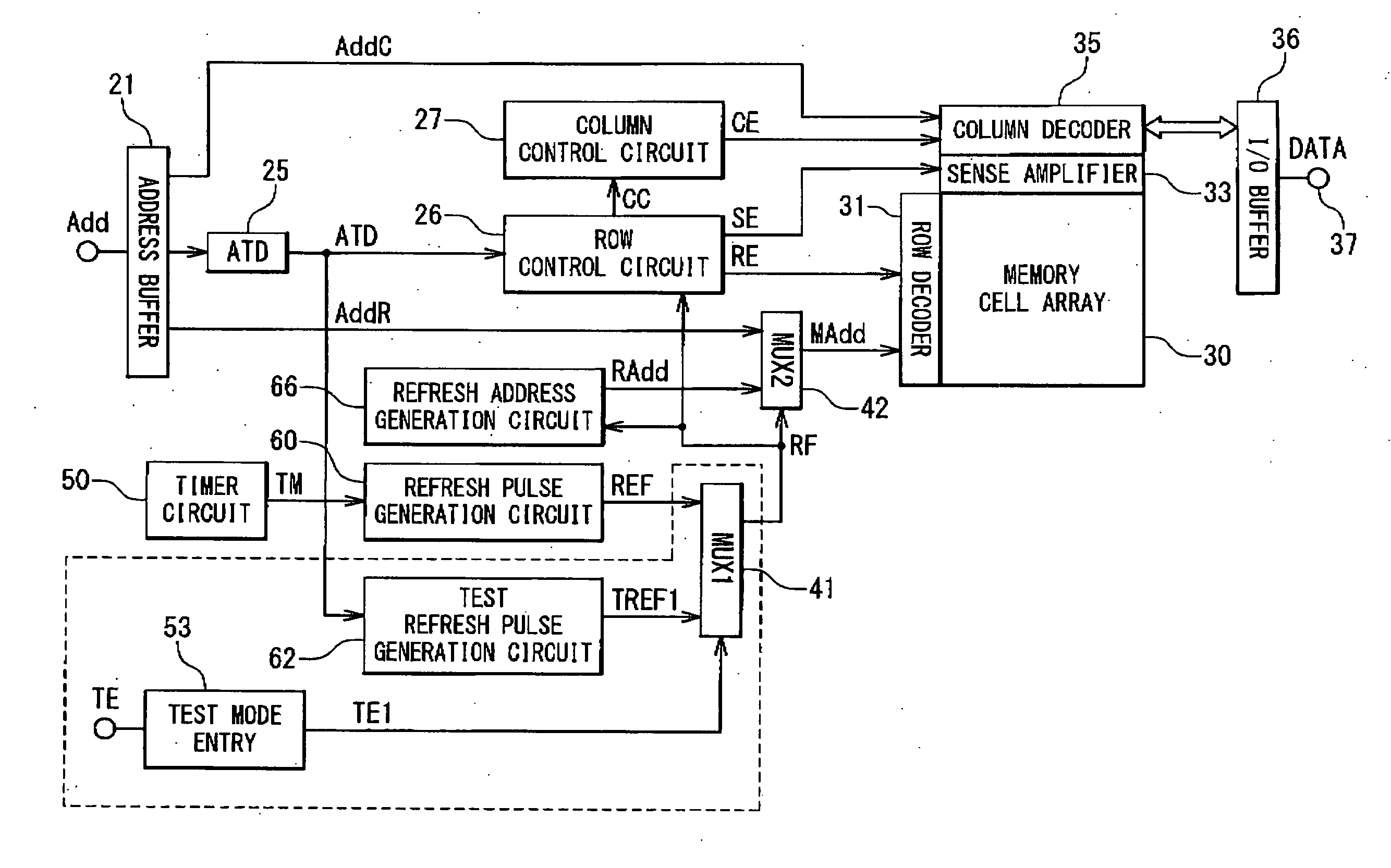
[0075]FIG. 3 is a block diagram showing a configuration of the pseudo SRAM according to a first embodiment of the present invention
[0076]The pseudo SRAM according to the first embodiment of the present invention contains a memory cell array unit 300, refresh control circuits (410, 50, 53, 60, 62 and 660) and access control circuits (210, 25, 250, 27, 35, 36 and 420). The memory cell array unit 300 contains a plurality of banks. The refresh control circuits (410, 50, 53, 60, 62 and 660) periodically output a refresh timing control signal RF. The access control circuits (210, 25, 250, 27, 35, 36 and 420) perform a self refresh operation (hereafter, referred to as the refresh operation) on non-adjacent bank groups, among the plurality of banks, in accordance with the combination of preset bank simultaneous activations and an activating order, when a refresh timing control signal RF is supplied.
[0077]The refresh control circuits (410, 50, 53, 60, 62 and 660) contain a switc...
second embodiment
Configuration
[0210]FIG. 11 is a block diagram showing the configuration of the pseudo SRAM according to the second embodiment of the present invention.
[0211]The pseudo SRAM according to the second embodiment of the present invention contains a row control circuit 2502 and a test mode entry circuit 532, instead of the row control circuit 250 and the test mode entry circuit 53 in the first embodiment. In the second embodiment, the descriptions overlapping with those of the first embodiment are omitted.
[0212]When a bank selection test mode entry signal TEB is given from outside, the test mode entry circuit 532 outputs the bank selection test mode entry signal TEB as a bank selection mode signal TSB to the row control circuit 2502, independently of a test mode entry signal TE.
[0213]FIG. 12 shows the configuration of the row control circuit 2502 in FIG. 11.
[0214]The row control circuit 2502 contains a bank activation allocation circuit 2902, instead of the bank activation allocation circ...
PUM
Abstract
In a large capacitysemiconductor storage device having a multi-bank configuration, it is desired to reduce a peak current of one refresh operation, to avoid an interference between adjacent banks, and to prevent a data breaking of a memory cell caused by a lack of a data hold time. A semiconductor storage device includes: a memory cell array part including a plurality of banks; a refresh control circuit configured to output a refresh timing control signal periodically; and an access control circuit configured to perform a refresh operation on a group of banks which are not adjacent to one another in accordance with a preset combination of banks which are simultaneously activated and a preset activating order when the refresh timing control signal is supplied.
Description
INCORPORATION BY REFERENCE[0001]This patent application is based on Japanese Patent Application No. 2009-163901. The disclosure of the Japanese Patent Application is incorporated herein by reference.BACKGROUND OF THE INVENTION[0002]1. Field of the Invention[0003]The present invention relates to a semiconductor storage device and a refresh control method of a semiconductor storage device.[0004]2. Description of Related Art[0005]In recent years, mobile devices represented by the mobile telephone include very many functions, and include a function for accessing WEB servers and displaying contents of websites on computer networks. In order to attain such functions, a large quantity of data received by the mobile device is required to be temporally stored in a semiconductor storage device inside the mobile device.[0006]As this semiconductor storage device, the SRAM (Static Random Access Memory) is preferable from the viewpoints that the treatment is easy, the operation speed is high, and...
Claims
Application Information
Patent Timeline
Application Date:The date an application was filed.
Publication Date:The date a patent or application was officially published.
First Publication Date:The earliest publication date of a patent with the same application number.
Issue Date:Publication date of the patent grant document.
PCT Entry Date:The Entry date of PCT National Phase.
Estimated Expiry Date:The statutory expiry date of a patent right according to the Patent Law, and it is the longest term of protection that the patent right can achieve without the termination of the patent right due to other reasons(Term extension factor has been taken into account ).
Invalid Date:Actual expiry date is based on effective date or publication date of legal transaction data of invalid patent.

