Forward converter with secondary side post-regulation and zero voltage switching

a converter and zero voltage technology, applied in the field of forward converters, can solve the problems of high switching losses, inability to achieve the zero voltage switching of the primary side switch transistor, and higher switching losses

Inactive Publication Date: 2011-01-20
GLACIALTECH +1
View PDF2 Cites 6 Cited by
  • Summary
  • Abstract
  • Description
  • Claims
  • Application Information

AI Technical Summary

Benefits of technology

[0019]the controllable switch is driven by the secondary side PWM control circuit. The freewheeling synchronous rectifier may be driven by the secondary side PWM control circuit or the secondary side driving winding. If the freewheeling synchronous rectifier is driven by the secondary side PWM control circuit, the dotted terminal of the secondary side driving winding connects to the gate of the forward synchronous rectifier through the forward gate resistor; the un-dotted terminal of the secondary side driving winding connects to the secondary ground terminal; as well as the forward gate-source resistor connects to the gate and the source of the forward

Problems solved by technology

Although very facile, the abovementioned primary side pre-regulation can not achieve zero-voltage switching of primary side switch transistors and suffers from higher switching losses.
is a higher positive voltage as well as both Q1 and Q2 are

Method used


Image

  • Forward converter with secondary side post-regulation and zero voltage switching
  • Forward converter with secondary side post-regulation and zero voltage switching
  • Forward converter with secondary side post-regulation and zero voltage switching

Examples


fourth embodiment

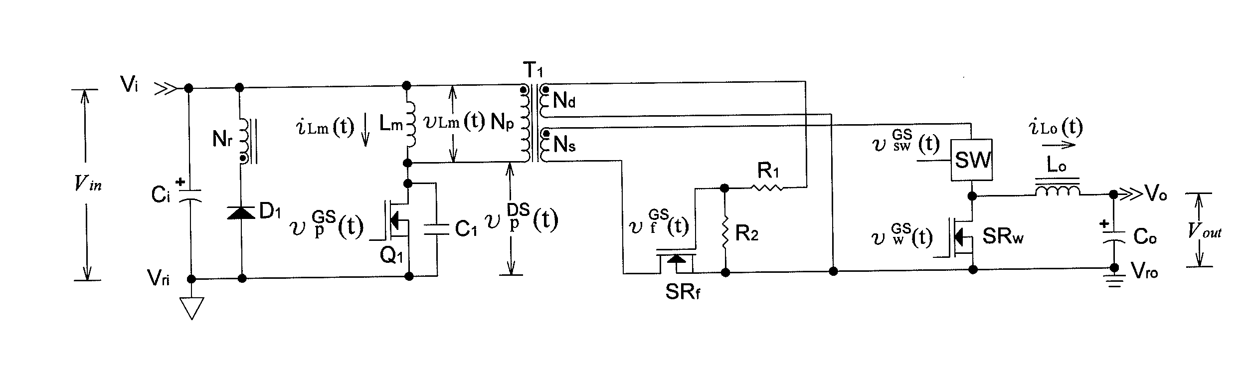
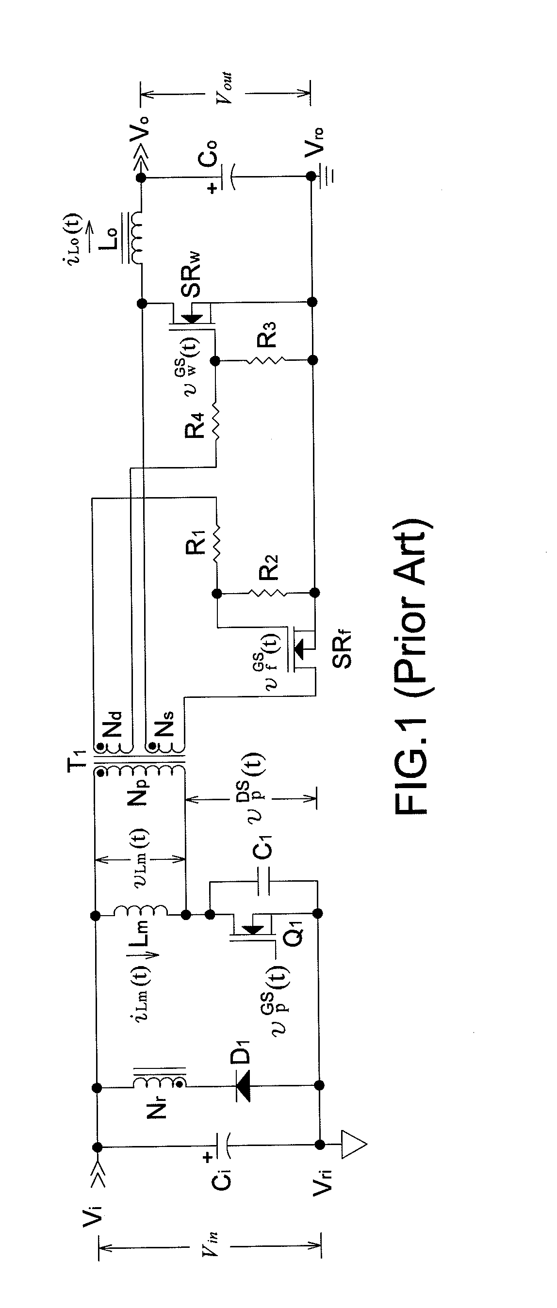
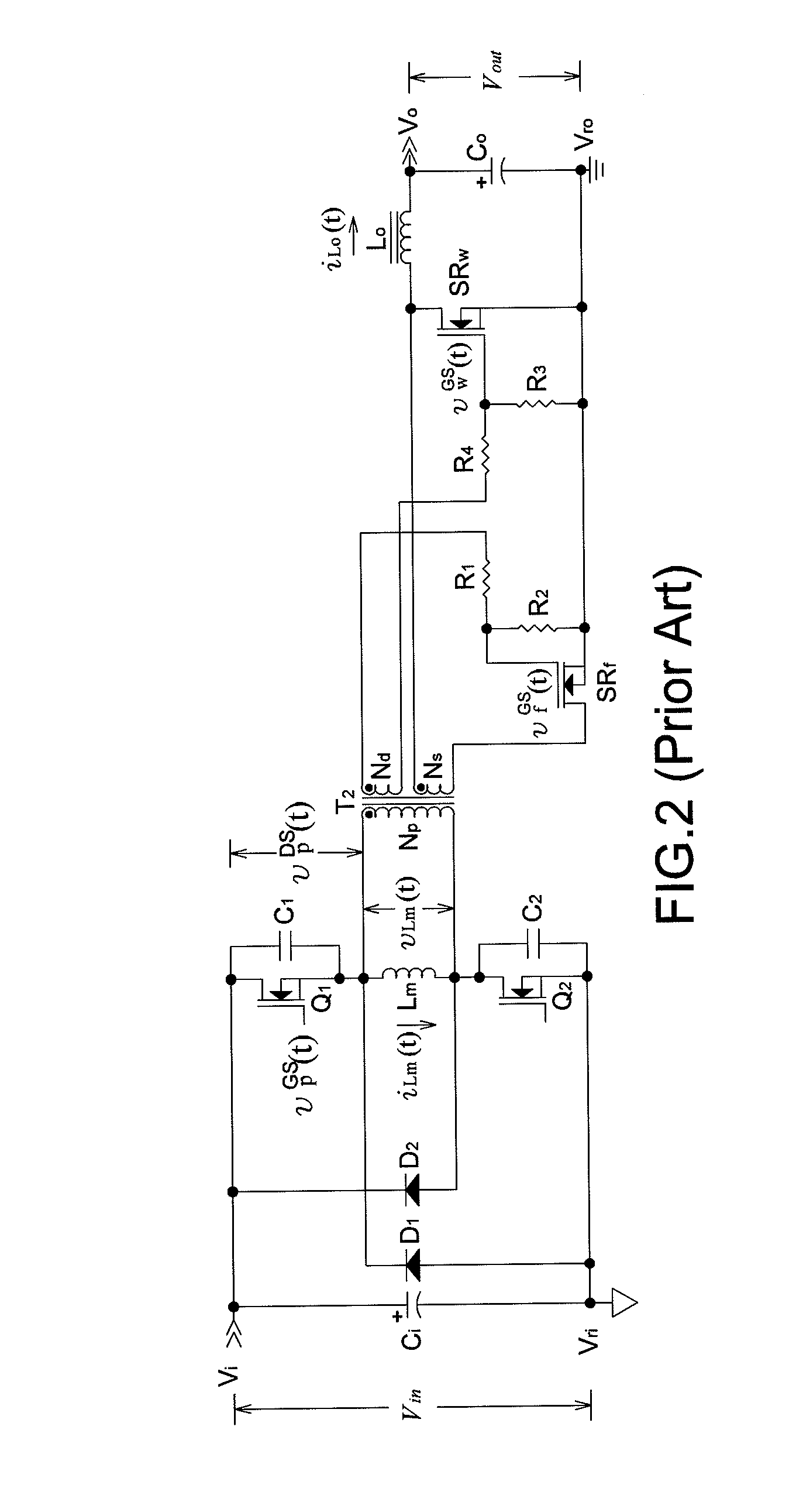
[0027]FIGS. 4, 5, 7, and 8 respectively depict main frames of a first, a second, a third and, a fourth embodiment based on the present invention. A secondary side error amplification circuit not shown therein detects a sample of the output voltage and compares the sample voltage with a reference voltage to generate an error signal fed back to a secondary side PWM control circuit not shown therein and converted into a PWM driving signal of a secondary side controllable switch for regulating the output voltage.

[0028]If D*pri is a constant primary duty ratio of primary side switch transistors, the output voltage Vout is expressible as

Vout=NsNpDsecVin,

wherein Vin is the input voltage; Np is the turns number of the primary side power winding; Ns is the turns number of the secondary side power winding; and Dsec≦D*pri is a variable secondary duty ratio of a secondary side controllable switch. A variable leading edge blanking time Tblank is expressible as Tblank=(D*pri−Dsec)Ts, wherein Ts i...

second embodiment

[0040]Since vpDS(t0·−)=0 as well as both Q1 and Q2 are switched on again at t=t0·to discharge vpDS(t0·)=0 , the first and the present invention can properly achieve zero voltage switching of primary side switch transistors to reduce switching losses.

[0041]FIG. 9 depicts crucial waveforms of FIG. 8 during a switching period, wherein SRw is driven by Nd.

[0042]During the interval of t0≦t1, vpGS(t) is high; the channels of Q1 and Q2 are both on; vpDS(t)=0; both D1 and D2 are off due to reverse biases; vLm(t)=Vin−2vpDS(t)=Vin; Lm is clamped to Vin and magnetized by iLm(t) flowing through the channel of Q2, Ci, and the channel of Q1; iLm(t) is increasing linearly with a positive slope

iLm(t)t=VinLm;

the induced voltage across Nd makes vfGS(t)>0 and vwGS(t)f is on and the channel of SRw is off. According to vswGS(t) provided by the secondary side PWM control circuit, this interval can be further subdivided into two subintervals:

During the subinterval of t0≦t02, SW switches off its channel to...


PUM


Abstract

The present invention discloses a forward converter with secondary side post-regulation and zero voltage switching, where the primary side power loop may adopt a single or a dual transistor structure, driven by a primary side driving circuit with a constant duty ratio so that the voltage waveform across the secondary side power winding has a constant pulse width; the secondary side power loop uses a controllable switch, a magnetic amplifier (MA) or an N channel metal oxide semiconductor field transistor (NMOS), to blank the leading edge of the voltage waveform across the secondary side power winding, regulate the output voltage, and achieve zero voltage switching of primary side switch transistors.

Description

FIELD OF THE INVENTION[0001]The present invention generally relates to a forward converter, and more particularly to a forward converter with secondary side post-regulation and zero voltage switching, achieving zero voltage switching of primary side switch transistors while post-regulating the output voltage at the secondary side.DESCRIPTION OF THE RELATED ART[0002]FIGS. 1 and 2 respectively depict conventional main frames of a single and a dual transistor forward converter having primary side pre-regulation and self-driven synchronous rectifiers, wherein a secondary side error amplification circuit not shown therein detects a sample of an output voltage and compares the sample voltage with a reference voltage to generate an error signal optically coupled to a primary side control circuit and converted into Pulse Width Modulation (PWM) driving signals of primary side switch transistors for regulating the output voltage.[0003]If the conventional forward converter operates in Continuo...

Claims


Application Information

Patent Timeline
IPC IPC(8): H02M3/335
CPCH02M3/33576
Inventor WANG, CHIH-LIANGYU, CHING-SHENG
Owner GLACIALTECH
Why Eureka
Try Eureka