Multi-layered electro-optic devices

a multi-layer electro-optic and optical technology, applied in the direction of instruments, color/spectral property measurements, material analysis, etc., can solve the problem of limited conversion efficiency of solar power into electricity of this device to a maximum of about 37%

Inactive Publication Date: 2011-02-03
SUNLIGHT PHOTONICS
View PDF65 Cites 215 Cited by
  • Summary
  • Abstract
  • Description
  • Claims
  • Application Information

AI Technical Summary

Problems solved by technology

The conversion efficiency of solar power into electricity of this device is limited to a maximum of about 37%, since photon energy in excess of the semiconductor's bandgap is wasted as heat.

Method used


Image

  • Multi-layered electro-optic devices
  • Multi-layered electro-optic devices
  • Multi-layered electro-optic devices

Examples


examples

[0063

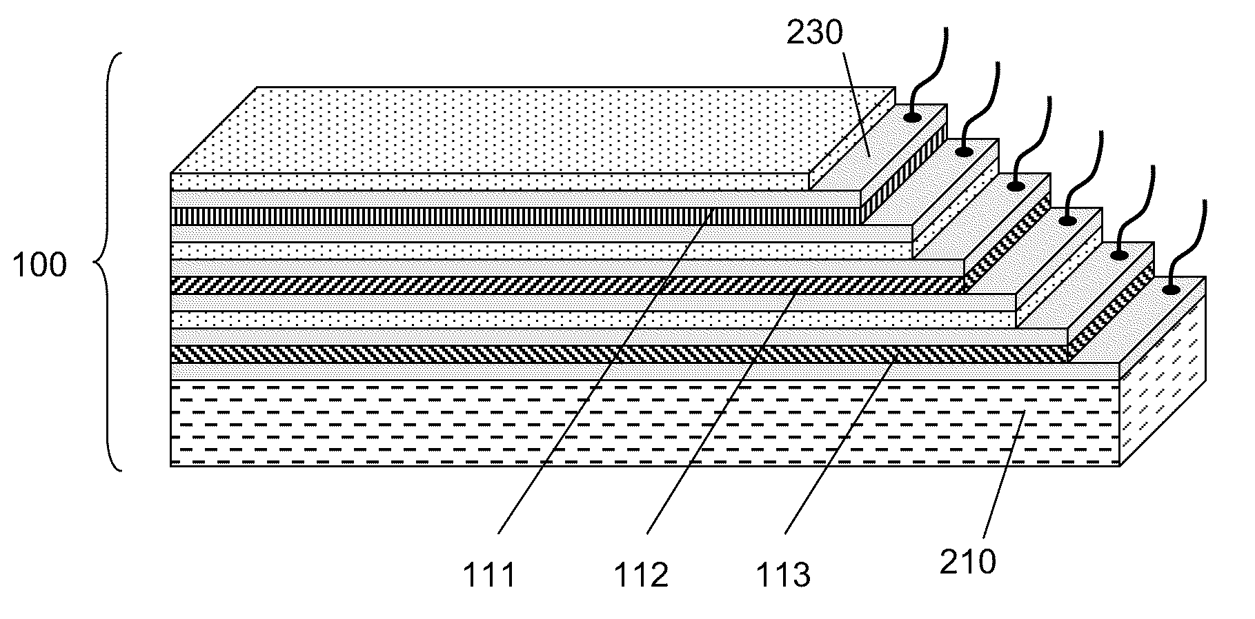
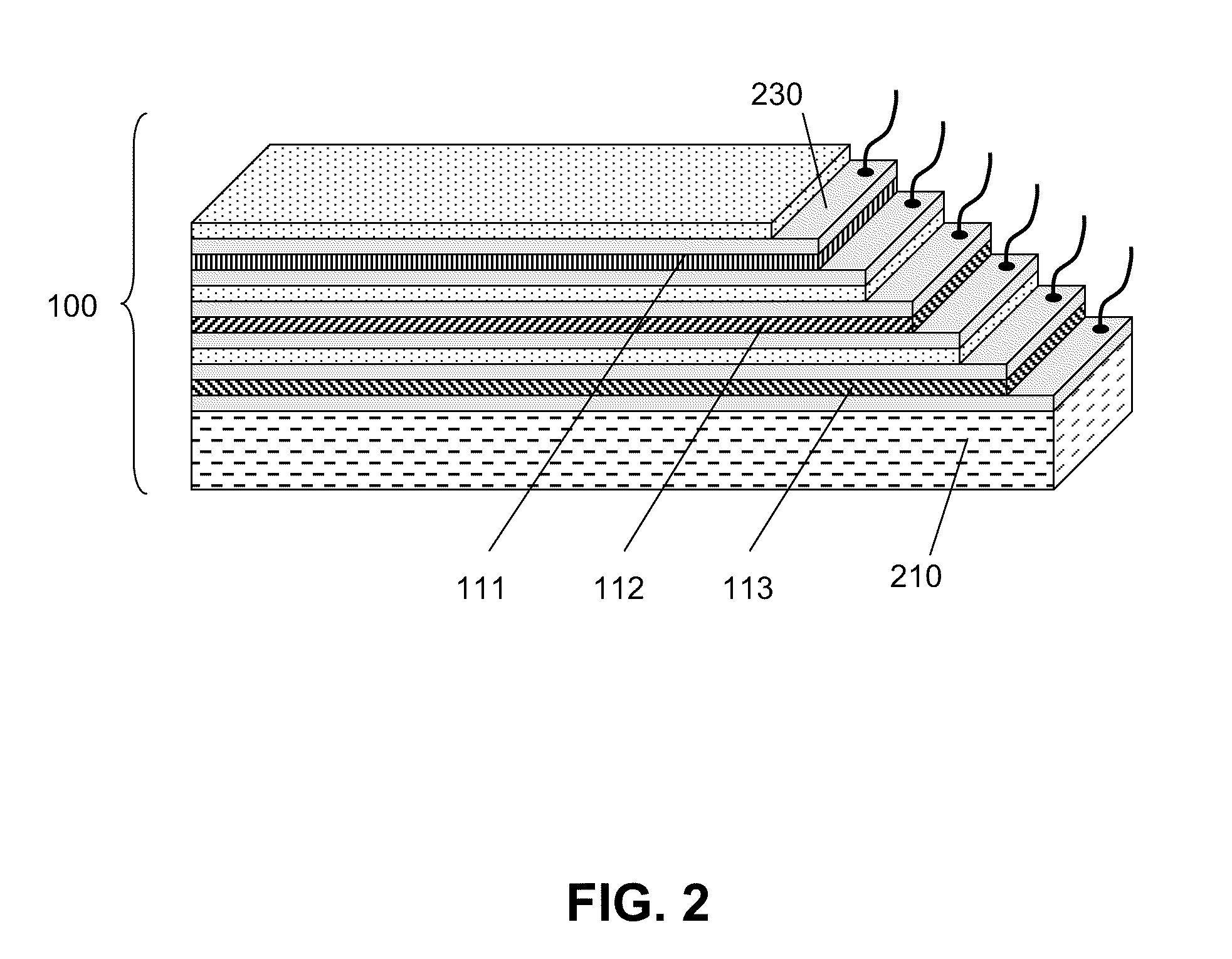
[0064]FIG. 2 shows an exemplary embodiment of the invention, in which three different photovoltaic modules 111, 112 and 113 are utilized. Maximum sunlight power conversion efficiency of this architecture is about 56% for highly concentrated sunbeam and about 50% for regular sunlight intensity (so called condition AM 1.5). All three modules contain active polycrystalline semiconductor materials based on, for example, a CIGS (Copper Indium Gallium Selenide) material system or a related alloy, and the corresponding junctions are produced using single junction designs known in the art. By varying the In and Ga relative concentrations the bandgaps in layer 111 may be adjusted to about 1.7 eV, in layer 112—to about 1.4 eV and in layer 113—to about 1.1 eV. The thickness of each layer may be in the range of 1 to 5 microns. Each module may also contain buffer layers, such as, for example, a thin CdSe layer with a thickness in the range of 10 to 1000 nm. The semiconductor layers in each ...


PUM


Abstract

A laminate film includes a plurality of planar photovoltaic semi-transparent modules disposed one on top of another and laminated to each other. Each of the modules includes a substrate, first and second conductive layers and at least first and second semiconductor layers disposed between the conductive layers. The first and second semiconductor layers define a junction at an interface therebetween. At least one of the junctions is configured to convert a first spectral portion of optical energy into an electrical voltage and transmit a second spectral portion of optical energy to another of the junctions that is configured to convert at least a portion of the second spectral portion of optical energy into an electrical voltage.

Description

CROSS REFERENCE TO RELATED APPLICATION[0001]The present application is a divisional of U.S. Ser. No. 12 / 034,883, filed Feb. 21, 2008, the contents of which are incorporated herein by reference.[0002]This application is also related to U.S. patent application Ser. No. 12 / 034,944, filed Feb. 21, 2008 and U.S. Ser. No. 12 / 777,392, filed May 11, 2010 (Attorney Docket Nos. 2800 / 3 and 2800 / 3D1), entitled “Method and Apparatus for Manufacturing Multi-Layered Electro-Optic Devices”, which is incorporated by reference in its entirety herein.BACKGROUND OF THE INVENTION[0003]1. Field[0004]The present invention relates generally to electro-optic devices and more particularly to electro-optic devices that have multiple layers and which can be produced by laminating or otherwise integrating two or more discrete electro-optic units or modules.[0005]2. Related art[0006]Photovoltaic devices represent one of the major sources of environmentally clean and renewable energy. They are frequently used to ...

Claims


Application Information

Patent Timeline
Patent Type & Authority Applications(United States)
IPC IPC(8): H01L31/02H01L33/08H05B44/00
CPCY02E10/50H01L31/043H01L2924/0002H01L2924/00H05B45/00G01N21/255G01N21/27
Inventor FROLOV, SERGEYCYRUS, MICHAEL
Owner SUNLIGHT PHOTONICS
Why Eureka
Try Eureka