Organic el device

a technology of organic el and light output, which is applied in the field of organic el devices, can solve the problems of insufficient increase of an overall light output, and achieve the effect of increasing light output and improving overall light outpu

Active Publication Date: 2011-02-03
SAMSUNG DISPLAY CO LTD
View PDF6 Cites 56 Cited by
  • Summary
  • Abstract
  • Description
  • Claims
  • Application Information

AI Technical Summary

Benefits of technology

[0021]The organic EL device in this arrangement allows the light-transmitting electrode 3 to be disposed on the smooth surface of the smoothing layer 11, without contact with a bumpy surface from which the dispersion particles 6 projects. It enables to form the light-transmissive electrode 3 having uniform thickness, without causing short-circuit at the light-transmissive electrode 3.
[0022]As described above, the organic EL device in the present invention emits light from the organic light emitting layer 2 and propagates out the light through the light dispersion layer 5 of the light guiding layer 4 a...

Problems solved by technology

But, this organic EL device decreases light output in the f...

Method used


Image

  • Organic el device
  • Organic el device
  • Organic el device

Examples


example 1

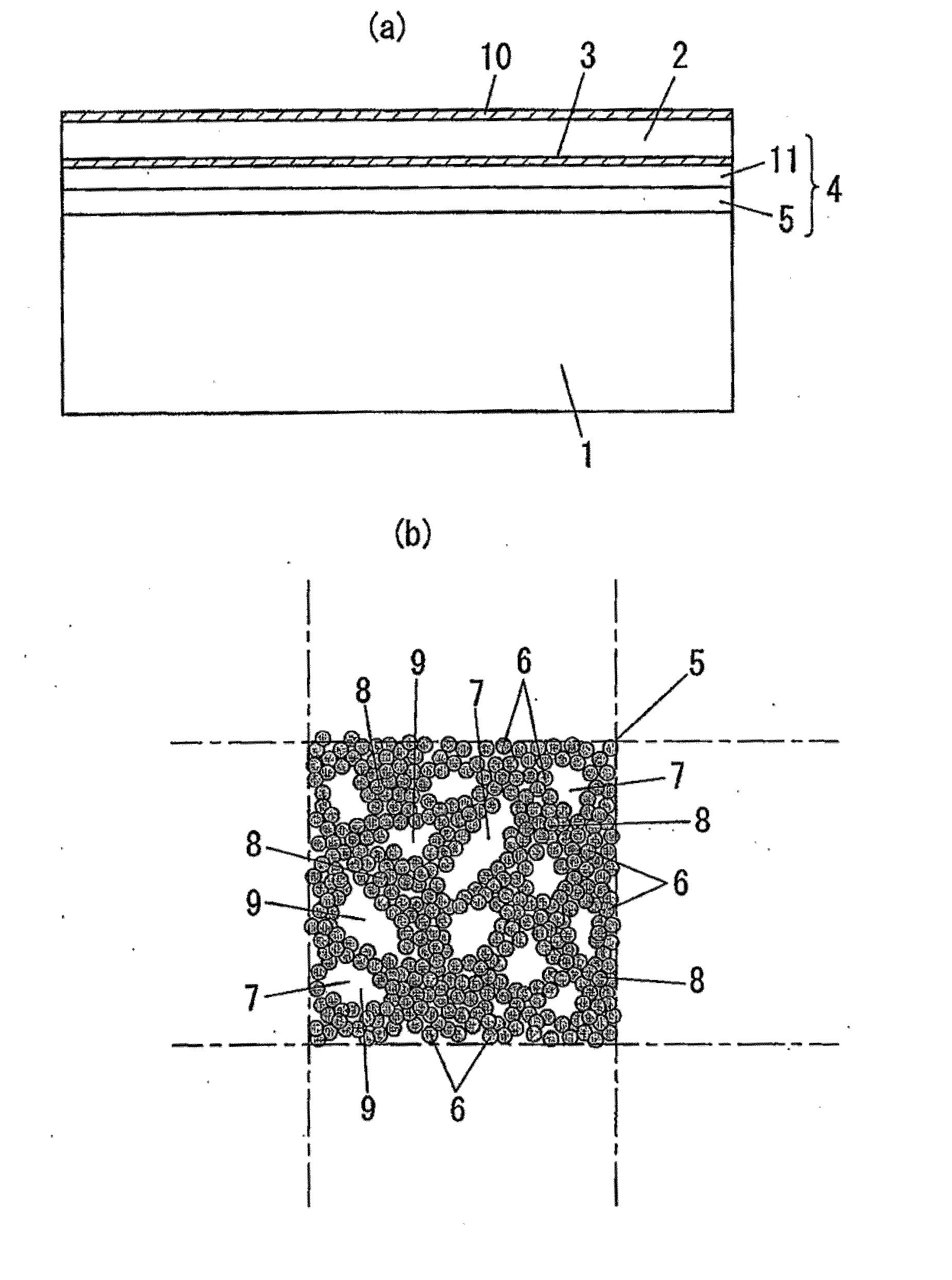
[0067]86.8 parts by weight of tetraethoxysilane, 34.7 parts by weight of γ-methacrylloxypropyltrimethoxysilane, and 75 parts by weight of 0.1N-nitric acid were added to 803.5 molecular weight of isopropylalcohol, and then sufficiently mixed with each other by using disper to give a solution. The resultant solution was stirred for two hours with being kept in thermostat bath at 40° C., giving 5-percent solution by weight of silicone resin having a weight-average molecular weight of 1050. Subsequently, the silicone resin solution was mixed with methylsilicone particles (available from GE Toshiba silicone Co. Ltd as “Tospal 120” having a mean diameter of 2 μm) as light dispersion particles 6, such that the ratio of methylsilicone particles / silicone resin was controlled at 80 / 20 in weight of solid content (a corresponding value of condensed compound, provided that Si is substituted with SiO2 in tetraalkoxysilane or with SiO1.5 in trialkoxysilane). The resultant mixture was dispersed...

example 2

[0074]The coating material was applied on the substrate 1 by spin-coater and then dried in the same way as in Example 1 repeatedly ten times to form the light dispersion layer 5. Thickness of the light dispersion layer 5 was measured by using contact surface profilometer (available from Japan Veeco Co. Ltd. as “DekTak3”). The mean thickness of the light dispersion layer 5 is about 8 μm. The surface of this light dispersion layer 5 was observed by using optical microscope (available from Keyence Co. Ltd. as “VHX-500”). FIG. 3 shows an optical microscopic photograph of surface of this light dispersion layer 5, with 500-fold magnification. As shown in FIG. 3, the light dispersion particles 6 almost wholly occupy within the light dispersion layer 5 (the light-transmissive region 9 has a dimension of less than 1 μm). The light dispersion layer 5 is formed with the light dispersion region 8 and the light-transmissive region 9. The light dispersion region 8 occupies about 90 percent of the...

example 3

[0076]The coating material was applied on the substrate 1 by spin-coater and then dried in the same way as in Example 1 only one time, so as to provide the light dispersion layer 5. Thickness of the light dispersion layer 5 was measured by using the contact surface profilometer (available from Japan Veeco Co. Ltd. as “DekTak3”). The mean thickness of the light dispersion layer 5 is about 1 μm. The surface of this light dispersion layer 5 was observed by using optical microscope (available from Keyence Co. Ltd. as “VHX-500”). FIG. 4 shows an optical microscopic photograph of the surface of this light dispersion layer 5, with 500-fold magnification. As shown in FIG. 4, the light-transmissive region 9 containing no light dispersion particles 6 almost wholly occupies the light dispersion layer 5, which contains only a fraction of the light dispersion region 8 filled with the aggregated light dispersion particles 6. The light dispersion layer 5 has a sea-islands structure, in which the l...


PUM


Abstract

An organic EL device in the present invention comprises a light-transmissive substrate 1, an organic light emitting layer 2, a light-transmissive electrode 3 disposed between the light-transmissive substrate 1 and the organic light emitting layer 2, and a light guiding layer 4 which is disposed between the substrate 1 and the light-transmissive electrode 3. The light guiding layer 4 is configured to alter light direction. The organic EL device is configured to emit light from the organic light emitting layer 2, and allow the light to propagate out through said light guiding layer 4, the light-transmissive electrode 3, and the light-transmissive substrate 1. The light guiding layer 4 includes a light dispersion layer 5. The light dispersion layer 5 is formed with a light dispersion region 8 and a light-transmissive region 9, which are arranged in a coplanar relation within said light dispersion layer 5. The light dispersion region 8 contains light dispersion particles 6 and a binder resin 7. The light-transmissive region 9 contains the light dispersion particles 6 at a lower ratio than the light dispersion region 8. The organic EL device in the present invention enables to improve an overall light output by suppressing the reduction of light output in the front direction as well as increasing light output in diagonal directions.

Description

TECHNICAL FIELD[0001]This invention relates to an organic EL device for utilized as liquid-crystal backlight, illumination device, various displays, and so on.BACKGROUND ART[0002]Organic EL device (organic electroluminescent device) has been developing as a typical surface illuminator. The organic EL device shown in FIG. 1(a) comprises a light-transmissive substrate 1, a light-transmissive electrode 3, an organic light emitting layer 2 made of an organic EL material, and a light-reflective opposing electrode 10, which are superimposed in this order. When receiving a voltage between the light-transmissive electrode 3 and the opposing electrode 10, the organic EL device emits light from the light emitting layer 2 to be output through the light-transmissive electrode 3 and the light-transmissive substrate 1.[0003]The organic EL device outputs the light which is emitted from the light emitting layer 2 through the light-transmissive electrode 3 and the light-transmissive substrate 1, but...

Claims


Application Information

Patent Timeline
IPC IPC(8): H01L51/50
CPCB82Y20/00H01L2251/5369H01L51/5268B82Y30/00H10K50/854H10K2102/331Y10S428/917
Inventor NAKAMURA, MASAHIROYAMAKI, TAKEYUKIMITSUTAKE, YOSHIOYAMANA, MASAHITOIDE, NOBUHIROITO, NORIHIROTSUJI, HIROYA
Owner SAMSUNG DISPLAY CO LTD
Why Eureka
Try Eureka