
Pixel structure and organic light emitting display using the same

Inactive Publication Date: 2011-02-03
SAMSUNG MOBILE DISPLAY CO LTD
View PDF3 Cites 65 Cited by
  • Summary
  • Abstract
  • Description
  • Claims
  • Application Information

AI Technical Summary

Benefits of technology

[0010]It is therefore a feature of an embodiment to provide a pixel structure adapted for higher definition and to have a relatively longer lifespan than comparable conventional pixels.
[0011]It is therefore a separate feature of an embodiment to provide an organic light emitting display including a pixel structure adapted for higher definition and to have a relatively longer lifespan than comparable conventional organic light emitting displays.
[0012]It is therefore a separate feature of an embodiment to provide a structure of a pixel having a reduced size, which may more easily enable higher resolution, relative to comparable conventional pixels.
[0013]It is therefore a separate feature of an embodiment to provide a structure of a pixel adapted to reduce an occurrence of black spots relative to comparable conventional pixels.
[0014]It is therefore a separate feature of an embodiment to provide a pixel and / or an organic light emitting display that is adapted to at least reduce an occurrence of black spots resulting from a blue emitting layer, which generally has a higher occurrence of black spots than a red or a green emitting layer, relative to comparable conventional pixels and displays.
[0015]It is therefore a separate feature of an embodiment to provide a pixel and / or an organic light emitting display that is adapted to have a longer lifespan by at least reducing color deterioration of the pixels over driving time.

Problems solved by technology

Currently, in general, blue emitting layers are more easily deteriorated and have a relatively shorter lifetime in comparison to other emitting layers.

Method used


Image

  • Pixel structure and organic light emitting display using the same
  • Pixel structure and organic light emitting display using the same
  • Pixel structure and organic light emitting display using the same

Examples


Embodiment Construction

[0043]Korean Patent Application No. 10-2009-0071278, filed on Aug. 3, 2009, in the Korean Intellectual Property Office, and entitled: “Pixel Structure and Organic Light Emitting Display Using the Same” is incorporated by reference herein in its entirety.

[0044]Exemplary embodiments will now be described more fully hereinafter with reference to the accompanying drawings; however, they may be embodied in different forms and should not be construed as limited to the embodiments set forth herein. Rather, these embodiments are provided so that this disclosure will be thorough and complete, and will fully convey the scope of the invention to those skilled in the art.

[0045]In the following detailed description, only certain exemplary embodiments of the present invention have been shown and described, simply by way of illustration. In the drawing figures, the dimensions of layers and regions may be exaggerated for clarity of illustration. Accordingly, the drawings and description are to be r...


PUM


Abstract

A pixel that is adapted for implementing higher definition and an organic light emitting display using such a pixel are provided. The pixel includes a red sub-pixel including a red emitting layer, a green sub-pixel including a green emitting layer, a first blue sub-pixel including a first blue emitting layer, and a second blue sub-pixel including a second blue emitting layer. The red emitting layer and the green emitting layer are symmetrically arranged and the first blue emitting layer and the second blue emitting layer are symmetrically arranged.

Description

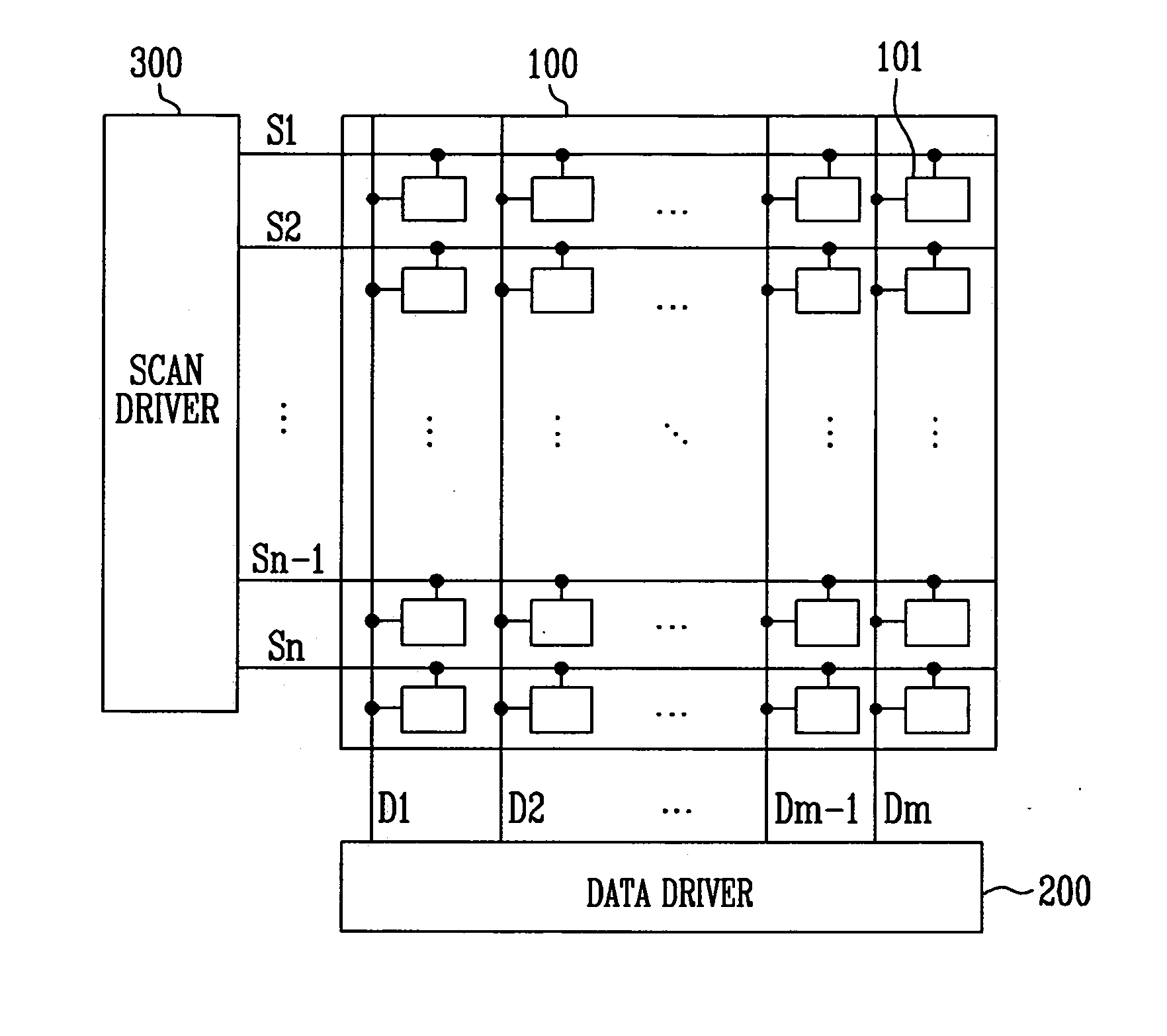
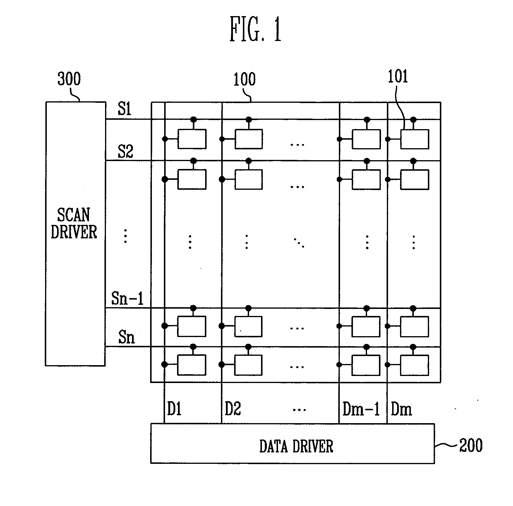
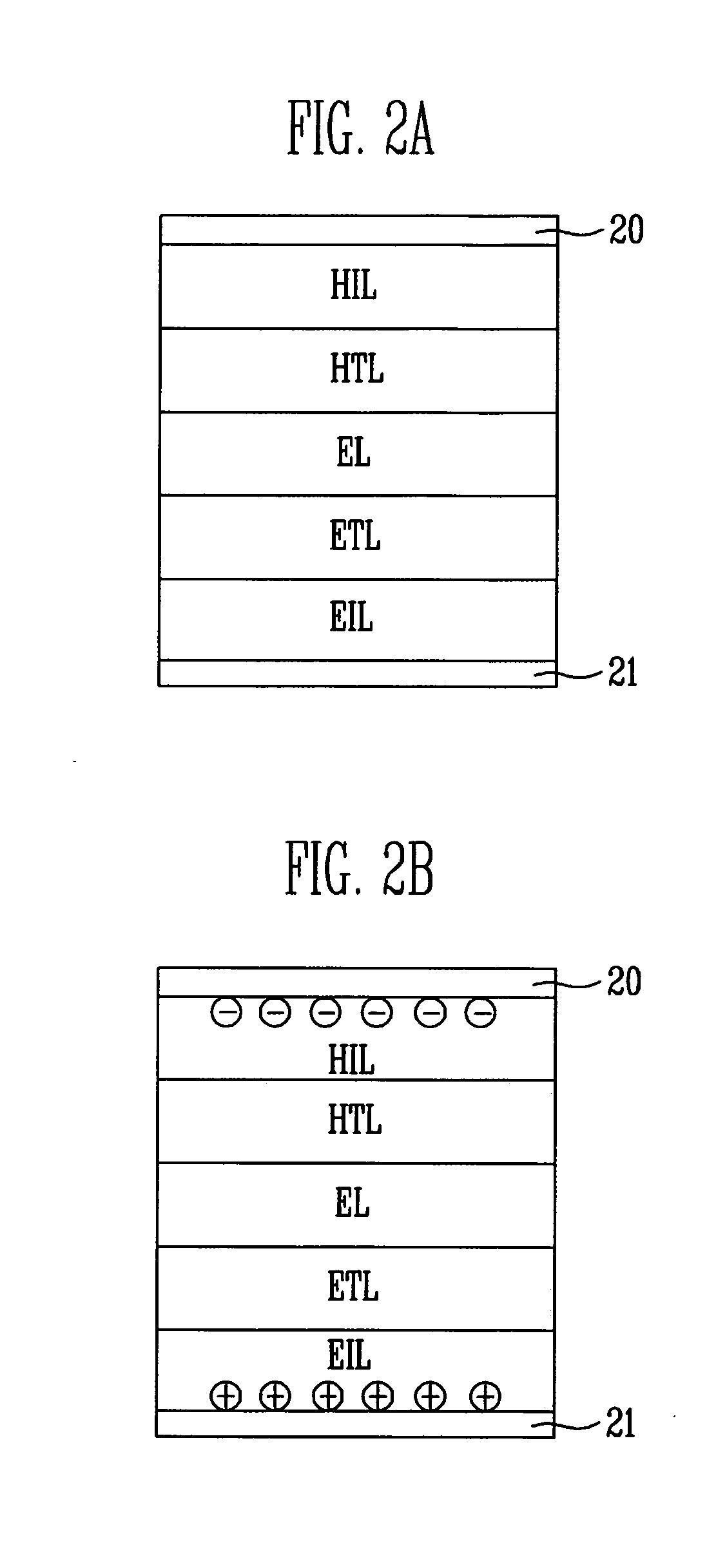
BACKGROUND[0001]1. Field[0002]Embodiments relate to a pixel structure and an organic light emitting display including such a pixel structure. More particularly, embodiments relate to a pixel structure capable of reducing a size of a light emitting unit of a pixel and an organic light emitting display including such a pixel structure.[0003]2. Description of the Related Art[0004]Organic light emitting flat panel displays, which are self emitting, adapted to employ low power, and lighter in weight and smaller in volume than cathode ray tubes are being employed instead of cathode ray tubes. There are various flat panel displays, e.g., liquid crystal displays (LCDs), field emission displays (FEDs), plasma display panels (PDPs), and organic light emitting diode (OLED) displays.[0005]Organic light emitting displays display an image using OLEDs, which generate and emit light as a result of recombination of electrons and holes.[0006]In general, OLED displays have various advantages, e.g., ex...

Claims


Application Information

Patent Timeline
IPC IPC(8): G09G5/10H01L33/36
CPCG09G3/3225H01L27/3218G09G2300/0452G09G2300/0443H10K59/353Y10S428/917
Inventor KIM, EUNAH
Owner SAMSUNG MOBILE DISPLAY CO LTD
Learn More