

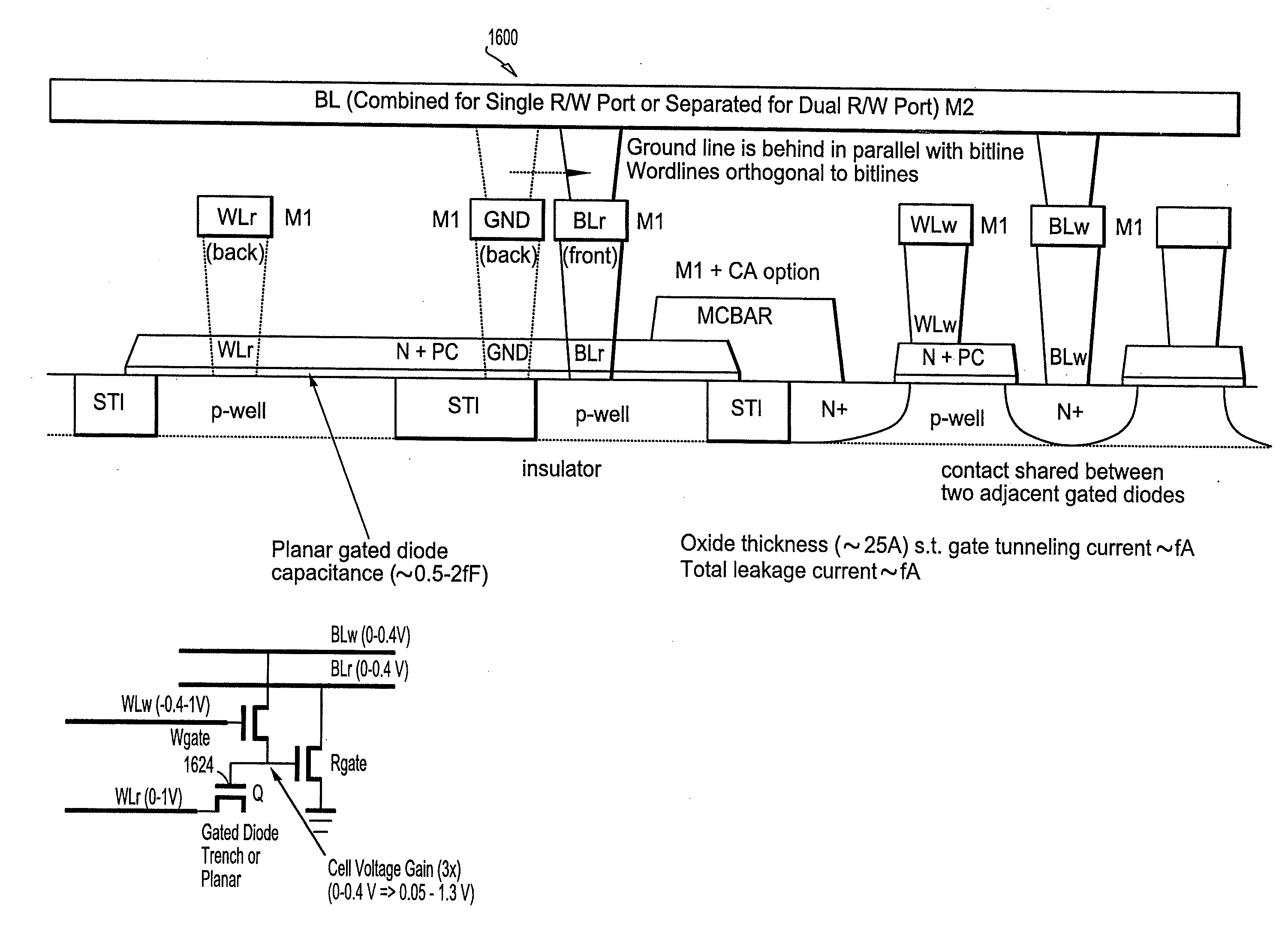
Gated Diode Memory Cells
a diode memory and gate technology, applied in the field of memory cells, can solve problems such as voltage drop in the cell
- Summary
- Abstract
- Description
- Claims
- Application Information
AI Technical Summary
Benefits of technology
Problems solved by technology
Method used
Image

Examples
Embodiment Construction
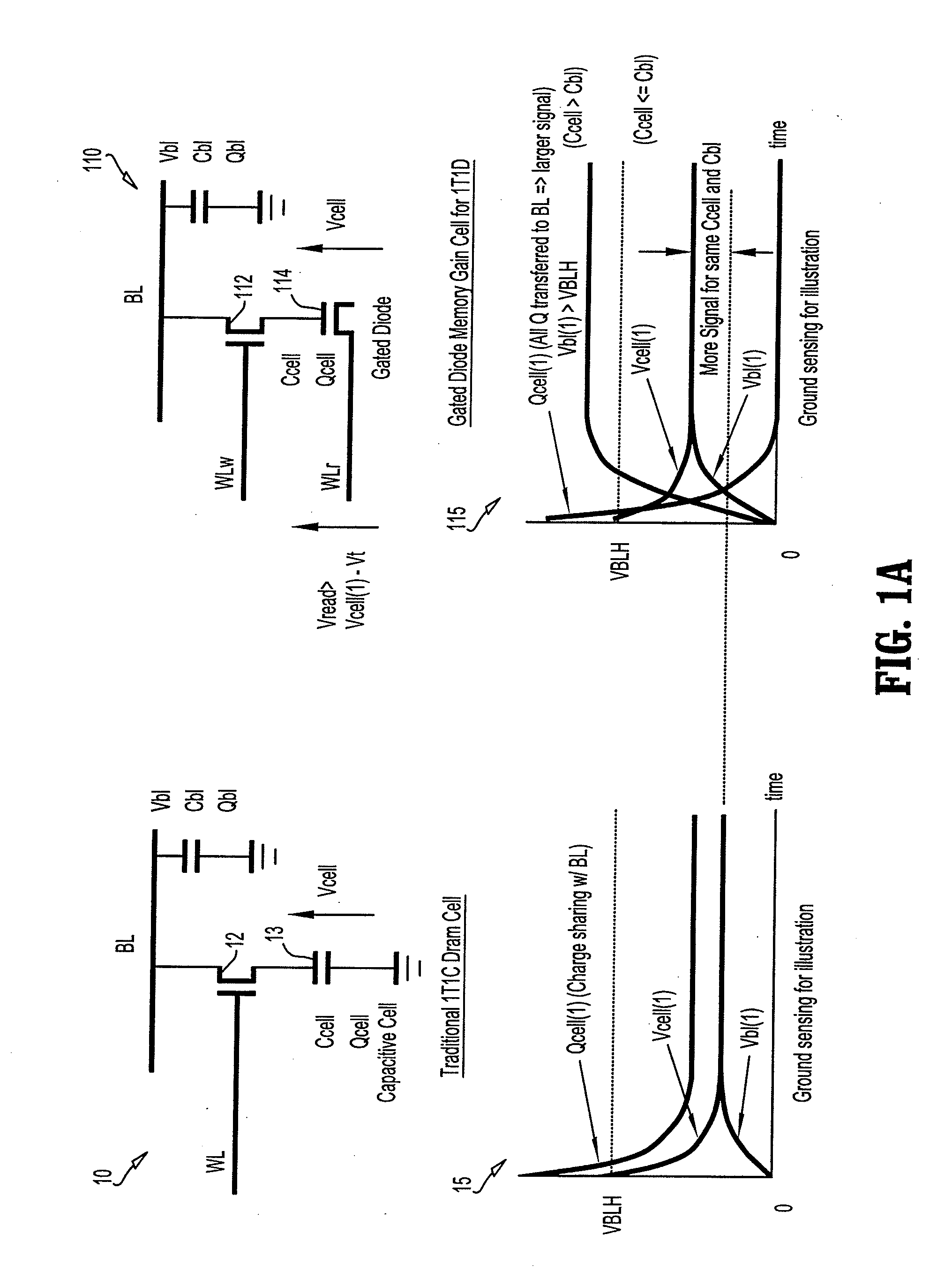
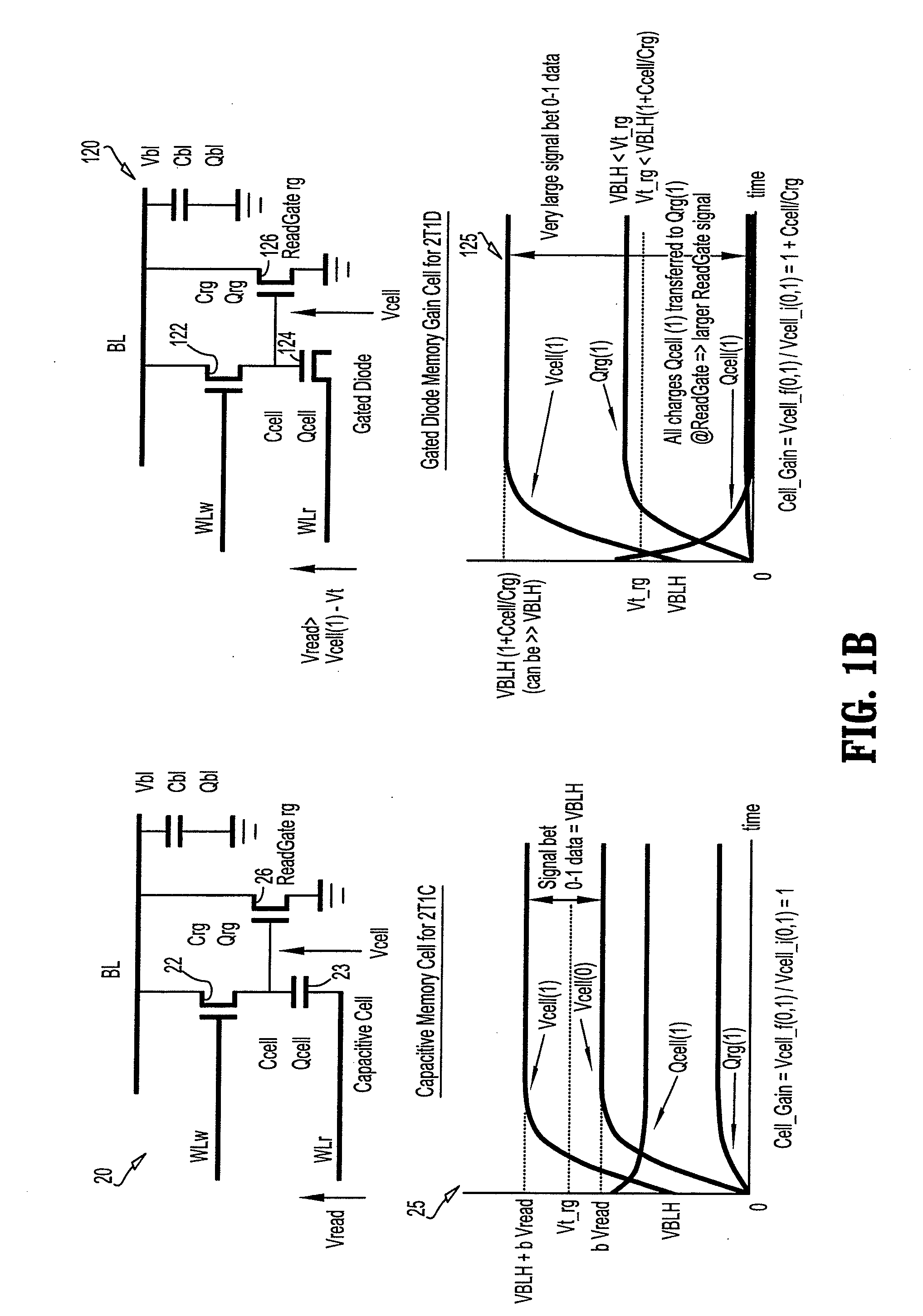
[0036]Traditionally, dynamic memory cells based on capacitors have exhibited voltage drops (such as 1T1C), or at best, a holding equal (such as 2T1C) during Read operations. A new memory cell is provided where the cell voltage can be increased during a Read operation, thereby significantly improving the sensing signal, sensing signal-to-noise ratio and sensing speed for dynamic memories built with cell structures according to the present disclosure. In the description that follows, the term “storage cell” refers to the gated diode, and the term “memory cell” refers to the whole 1T1D or the whole 2T1D device. The terms “implementing FET for the gated diode”, “gated diode implementing FET” or simply “gated diode FET” may be used interchangeably.
[0037]As shown in FIG. 1A, a Gated Diode Memory Gain Cell for a one-transistor one-diode (“1T1D”) DRAM cell is indicated generally by the reference numeral 110. The 1T1D DRAM cell 110 includes a transistor 112 in signal communication with a gat...
PUM
 Abstract
Description
Claims
Application Information