Substrate for mounting device and method for producing the same, semiconductor module and method for producing the same, and portable apparatus provided with the same

a semiconductor module and mounting device technology, applied in the direction of printed circuit assembling, printed circuit manufacturing, basic electric elements, etc., can solve the problems suppressing the miniaturization of a semiconductor module, and reducing the number of production processes. , the connection reliability between a projected structure and an electrode of a semiconductor device can be improved, and the effect of reducing the number of production processes

Inactive Publication Date: 2011-02-03
SANYO ELECTRIC CO LTD
View PDF24 Cites 16 Cited by
  • Summary
  • Abstract
  • Description
  • Claims
  • Application Information

AI Technical Summary

Benefits of technology

[0007]The present invention has been made in view of these situations, and a general purpose of the invention is to provide a technique in which further miniaturization of a semiconductor module can be achieved as well as reduction in the number of the production processes. Another purpose of the invention is to provide a technique in which the connection reliability between a projected structure and an electrode of a semiconductor device can be improved in the structure in which the two are connected to each other.

Problems solved by technology

However, in the flip-chip mounting method, there are limitations in narrowing the pitch between electrodes, because of restrictions resulting from the size of the solder bump itself and occurrence of bridges while soldering, or the like.
However, in the conventional semiconductor devices, there are problems that miniaturization of a semiconductor module is suppressed and the number of the production processes is increased, because a passive device such as a capacitor or the like is mounted on a silicon substrate as a separate part.
Further, in the structure in which a wiring layer of a substrate for mounting a device and a semiconductor device are made into one body via an insulating resin, such that a projected structure provided on the wiring layer and an electrode of the semiconductor device are connected, adhesion between the insulating resin and the semiconductor device is not high.
Therefore, there is a fear that the insulating resin could peel from the semiconductor device by a thermal stress generated due to, for example, a change in temperature of the environment.
And, in the case where the insulating resin peels from the semiconductor device, adhesion between the projected structure and the semiconductor device is decreased; and as a result, there is a fear that the connection reliability between the projected structure and the semiconductor device is decreased.

Method used


Image

  • Substrate for mounting device and method for producing the same, semiconductor module and method for producing the same, and portable apparatus provided with the same
  • Substrate for mounting device and method for producing the same, semiconductor module and method for producing the same, and portable apparatus provided with the same
  • Substrate for mounting device and method for producing the same, semiconductor module and method for producing the same, and portable apparatus provided with the same

Examples


embodiment 1

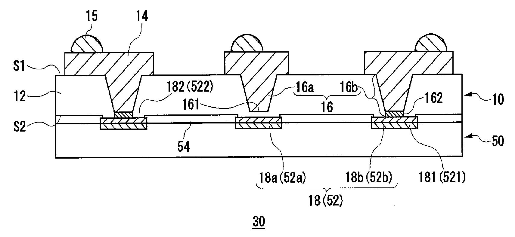
[0044]FIG. 1 is a schematic cross-sectional diagram illustrating a structure of a substrate 10 for mounting a device and a semiconductor module 30 using the same according to Embodiment 1. The semiconductor module 30 comprises the substrate 10 for mounting a device and a semiconductor device 50 mounted thereon.

[0045]The substrate 10 for mounting a device comprises: an insulating resin layer 12 formed by an insulating resin; a wiring layer 14 provided on one major surface S1 of the insulating resin layer 12; and a plurality of projected electrodes 16 that are connected to the wiring layer electrically, and that project toward the insulating resin layer 12 from the wiring layer 14. The substrate 10 for mounting a device is provided with a counter electrode 18 that is provided at a position corresponding to each of the plurality of projected electrodes 16 on the other major surface S2 of the insulating resin layer 12, and that has a counterface 181 facing the top face 161 of the projec...

embodiment 2

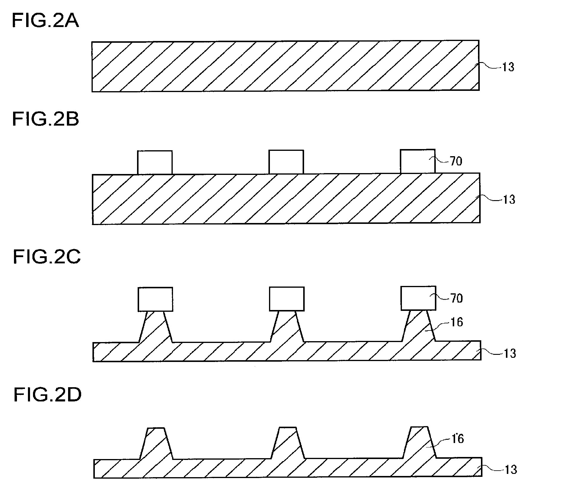
[0072]In the above Embodiment 1, the substrate 10 for mounting a device or the semiconductor module 30 is formed by subjecting the copper plate 13 and the counter electrode 18 or the semiconductor device 50 to pressure molding with the insulating resin layer 12 sandwiched between the two such that they are formed into one body; however, the substrate 10 for mounting a device or the semiconductor module 30 may also be formed in the following process. Hereinafter, the present embodiment will be described. It is noted that the projected electrode 16 is formed in the same way as with Embodiment 1, and the same structure as in Embodiment 1 is denoted with the same reference numeral as in Embodiment 1, and the description with respect thereto is omitted.

[0073]FIGS. 5A to 5F and FIGS. 6A to 6C are cross-sectional diagrams illustrating a method for connecting the projected electrode 16 and the counter electrode 18 or the device electrode 52.

[0074]As illustrated in FIG. 5A, a resist 71 is st...

embodiment 3

[0084]In the structures of the above Embodiments 1 and 2, the insulating resin layer 12 lies between the projected electrode 16a and the counter electrode 18a or the device electrode 52a; however, a dielectric film layer having a dielectric constant larger than that of the insulating resin layer 12 may be provided between the projected electrode 16a and the counter electrode 18a or the device electrode 52a, as illustrated in the present embodiment. Hereinafter, the present embodiment will be described. It is noted that the projected electrode 16 is formed in the same way as with Embodiment 1, and the same structure as in Embodiments 1 and 2 is denoted with the same reference numeral as in Embodiments 1 and 2, and the description with respect thereto is omitted.

[0085]FIGS. 7A to 7G and FIGS. 8A to 8E are cross-sectional diagrams illustrating a method for connecting the projected electrode 18 and the counter electrode 18 or the device electrode 52.

[0086]As illustrated in FIG. 7A, a di...


PUM

PropertyMeasurementUnit
temperatureaaaaaaaaaa
viscosityaaaaaaaaaa
dielectric constantaaaaaaaaaa

Abstract

A substrate for mounting a device comprises: an insulating resin layer; a plurality of projected electrodes that are connected electrically to a wiring layer provided on one major surface of the insulating resin layer, and that project toward the insulating resin layer from the wiring layer; and a counter electrode provided at a position corresponding to each of the plurality of projected electrodes on the other major surface of the insulating resin layer. Among the projected electrodes, a projected length of part of the projected electrodes is smaller than that of the other projected electrodes; and the projected electrode and the counter electrode corresponding thereto are capacitively-coupled, and the projected electrode and the counter electrode are connected electrically.

Description

CROSS-REFERENCE TO RELATED APPLICATIONS[0001]This application is based upon and claims the benefit of priority from the prior Japanese Patent Applications No. 2007-335819, filed Dec. 27, 2007, and Japanese Patent Application No. 2008-091664, filed Mar. 31, 2008, the entire contents of which are incorporated herein by reference.BACKGROUND OF THE INVENTION[0002]1. Field of the Invention[0003]The present invention relates to a substrate for mounting a device and a method for producing the same, a semiconductor module and a method for producing the same, and a portable apparatus provided with the same.[0004]2. Description of the Related Art[0005]Amid the acceleration of high performance of portable electronic apparatuses such as portable phone, PDA, DVC, and DSC, in order to be accepted in the market, it is essential that such products are miniaturized and reduced in their weight. Hence, there is also a demand for miniaturization of semiconductor modules such as multi-chip module (MCM) ...

Claims


Application Information

Patent Timeline
Patent Type & Authority Applications(United States)
IPC IPC(8): H01L21/50H05K3/02
CPCH01L21/486Y10T29/49156H01L23/48H01L23/49827H01L23/525H01L24/16H01L24/81H01L2224/0231H01L2224/13099H01L2224/81208H01L2224/81801H01L2224/81894H01L2224/83101H01L2924/01013H01L2924/01029H01L2924/01078H01L2924/01079H01L2924/14H01L2924/19041H05K3/4647H05K3/4652H05K2203/0369H01L2924/01005H01L2924/01006H01L2924/01033H01L2924/01047H01L2924/014H01L2224/02319H01L2224/0401H01L2924/13091H01L23/3114Y10T29/4913H01L2924/00H01L2924/351
Inventor SAITOU, KOUICHIOKAYAMA, YOSHIOTAKANO, YOHNAKASATO, MAYUMI
Owner SANYO ELECTRIC CO LTD
Why Eureka
Try Eureka