Radiation detector having a bandgap engineered absorber

a radiation detector and bandgap technology, applied in the field of imaging devices, can solve the problems of reducing the noise equivalent sensitivity of the device, and increasing the cost of cooling systems

Active Publication Date: 2011-02-10
DRS NETWORK & IMAGING SYST
View PDF4 Cites 30 Cited by
  • Summary
  • Abstract
  • Description
  • Claims
  • Application Information

AI Technical Summary

Problems solved by technology

Temperature affects dark current as higher temperature increases dark current and degrades the noise equivalent sensitivity of the device.
In addition, the cooling systems are necessarily larger and more expensive.
Such prior art infrared detectors employing photodiodes formed of HgCdTe are susceptible to noise due to thermally excited current carriers and dark current sources at high operating temperatures and, thus, require substantial cooling to reduce the operating temperature of the detector so as to correspondingly reduce the noise and dark current of the detector.

Method used


Image

  • Radiation detector having a bandgap engineered absorber
  • Radiation detector having a bandgap engineered absorber
  • Radiation detector having a bandgap engineered absorber

Examples


Embodiment Construction

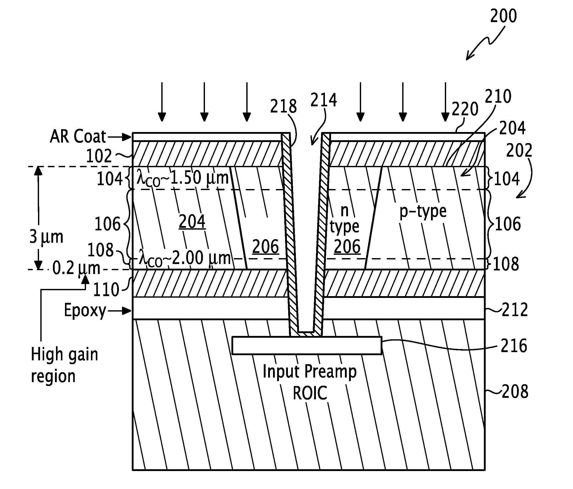
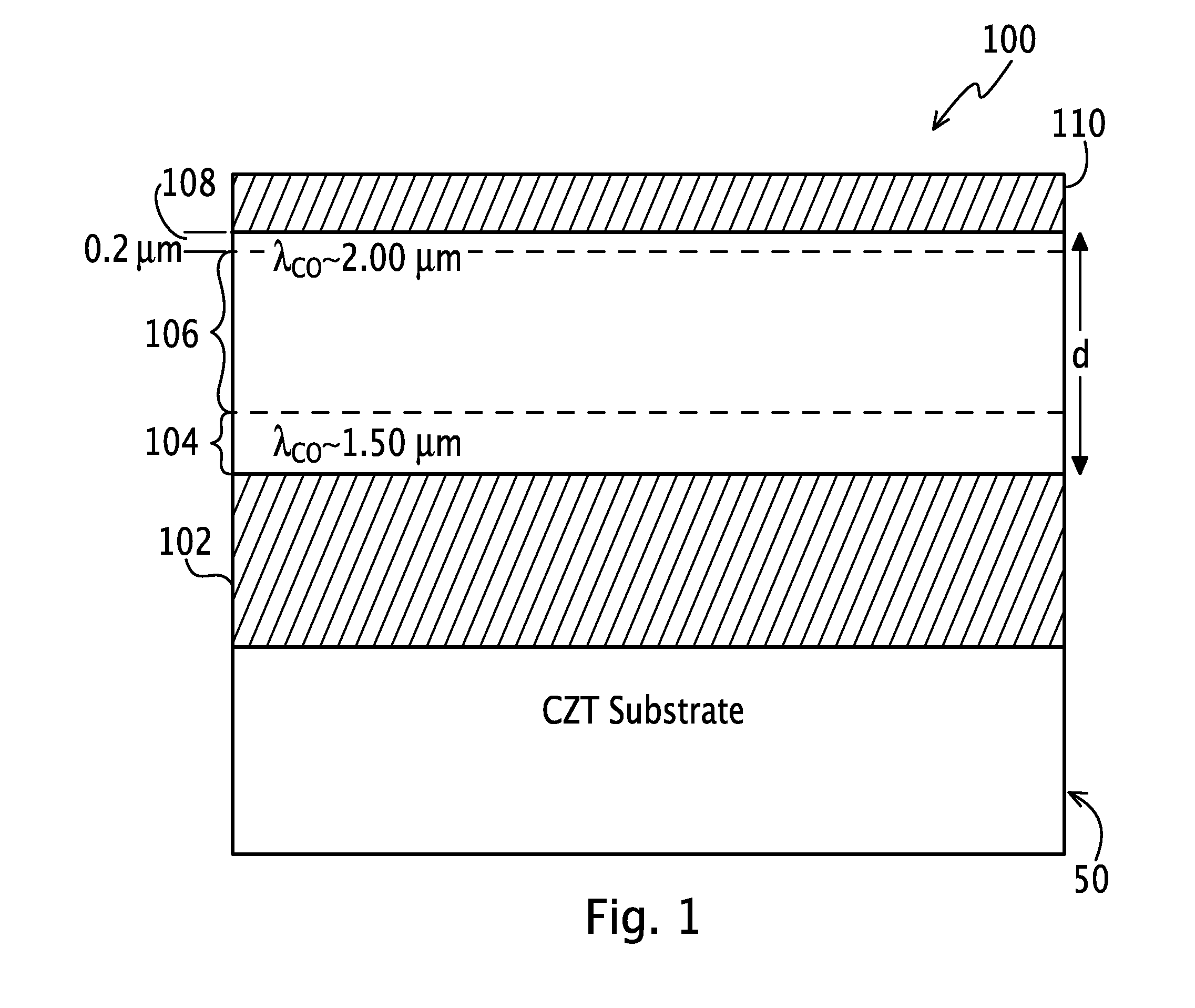
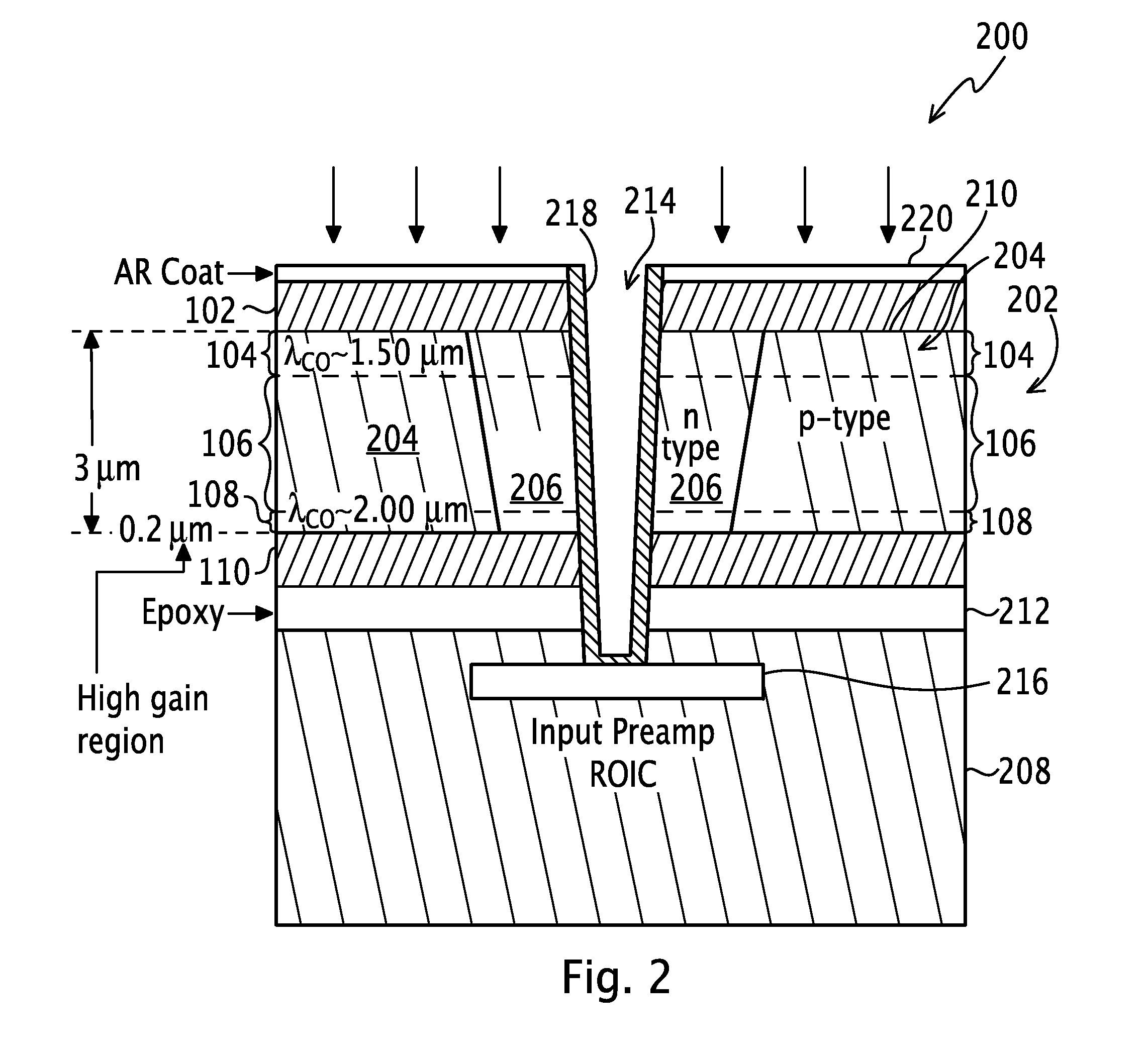
[0022]A photodiode is an electronic sensor that converts radiation into current or voltage signals. Imaging devices, such as photodiodes, consistent with the principles of the present invention may provide an HDVIP® radiation detector with an improved photodiode structure as an alternative to the conventional HDVIP® radiation detectors with photodiodes formed using liquid phase epitaxy (LPE) to have a single homogenous semiconductor layer of Hg1-xCdxTe with a given wavelength cutoff. The improved photodiode structure of the HDVIP® radiation detector reduces dark current densities as compared to the conventional HDVIP® radiation detector or increases the operating temperature of each pixel employing the structure and the focal plane array (FPA) of pixels as a whole. In one embodiment, the photodiode structure incorporates a thin, narrow bandgap layer beneath a thicker, larger bandgap layer having a bandgap engineered absorber, such as a graded composition of Hg1-xCdxTe. Carriers asso...


PUM


Abstract

A radiation detector is provided that includes a photodiode having a radiation absorber with a graded multilayer structure. Each layer of the absorber is formed from a semiconductor material, such as HgCdTe. A first of the layers is formed to have a first predetermined wavelength cutoff. A second of the layers is disposed over the first layer and beneath the first surface of the absorber through which radiation is received. The second layer has a graded composition structure of the semiconductor material such that the wavelength cutoff of the second layer varies from a second predetermined wavelength cutoff to the first predetermined wavelength cutoff such that the second layer has a progressively smaller bandgap than the first bandgap of the first layer. The graded multilayer radiation absorber structure enables carriers to flow toward a conductor that is used for measuring the radiation being sensed by the radiation absorber.

Description

FIELD OF THE INVENTION[0001]The principles of the present invention relate to imaging devices. More particularly, the principles of the present invention relate to a radiation detector, such as an infrared detector having a progressively graded bandgap or variable bandgap multilayer structure in which the detector's bandgap multilayer structure takes advantage of a longer cutoff region while minimizing the penalty associated with the added dark current of the longer cutoff region by confining this region to a thin layer within the graded or multilayer structure.BACKGROUND OF THE INVENTION[0002]Photodiodes have been configured in many ways and use many different materials for absorbing light energy over different wavelengths to generate photocurrent or voltage depending upon the mode. Temperature affects dark current as higher temperature increases dark current and degrades the noise equivalent sensitivity of the device. To achieve increased sensitivity, temperature is typically redu...

Claims


Application Information

Patent Timeline
Patent Type & Authority Applications(United States)
IPC IPC(8): G01J1/16H01L31/0296H01L31/18
CPCH01L31/02966H01L31/1832H01L31/02161H01L31/1032G01J5/046G01J5/024H01L27/1446H01L27/14652G01J5/0853H01L31/107G01J1/44H01L31/0232H01L31/024H01L31/101
Inventor MITRA, PRADIPBECK, JEFFREY D.SKOKAN, MARK R.
Owner DRS NETWORK & IMAGING SYST
Why Eureka
Try Eureka