Process for manufacturing MEMS devices having buried cavities and MEMS device obtained thereby

a technology of buried cavities and manufacturing processes, applied in the direction of microstructural devices, microstructure devices, acceleration measurement using interia forces, etc., can solve the problems of inability to use conformal materials, process is thus rather complex, and membranes (polysilicon layers over cavities) are perforated and thus fragil

Active Publication Date: 2011-02-10
STMICROELECTRONICS SRL
View PDF8 Cites 10 Cited by
  • Summary
  • Abstract
  • Description
  • Claims
  • Application Information

AI Technical Summary

Problems solved by technology

This process is thus rather complex on account of the operations of filling and emptying the cavity and the trenches.
In addition, the resulting membrane (polysilicon layer over the cavity) is perforated and thus fragile.
In fact, it is generally not possible to use a conformal material, otherwise this would penetrate into the cavity just obtained and would bring about at least partial filling thereof, with consequent false capacitive coupling.
On the other hand, the use of a non-conformal material, given also the geometrical characteristics of the holes, which are narrow and deep for the applications where a membrane of large thickness is required, does not generally enable complete closing thereof.
Also the use of two different materials, a first, non-co

Method used


Image

  • Process for manufacturing MEMS devices having buried cavities and MEMS device obtained thereby
  • Process for manufacturing MEMS devices having buried cavities and MEMS device obtained thereby
  • Process for manufacturing MEMS devices having buried cavities and MEMS device obtained thereby

Examples


Embodiment Construction

[0024]In the following description, numerous specific details are given to provide a thorough understanding of embodiments. The embodiments can be practiced without one or more of the specific details, or with other methods, components, materials, etc. In other instances, well-known structures, materials, or operations, for example; mask, are not shown or described in detail to avoid obscuring aspects of the embodiments.

[0025]Reference throughout this specification to “one embodiment” or “an embodiment” means that a particular feature, structure, or characteristic described in connection with the embodiment is included in at least one embodiment. Thus, the appearances of the phrases “in one embodiment”“according to an embodiment” or “in an embodiment” and similar phrases in various places throughout this specification are not necessarily all referring to the same embodiment. Furthermore, the particular features, structures, or characteristics may be combined in any suitable manner i...


PUM


Abstract

A process for manufacturing a MEMS device, wherein a bottom silicon region is formed on a substrate and on an insulating layer; a sacrificial region of dielectric is formed on the bottom region; a membrane region, of semiconductor material, is epitaxially grown on the sacrificial region; the membrane region is dug down to the sacrificial region so as to form through apertures; the side wall and the bottom of the apertures are completely coated in a conformal way with a porous material layer; at least one portion of the sacrificial region is selectively removed through the porous material layer and forms a cavity; and the apertures are filled with filling material so as to form a monolithic membrane suspended above the cavity.

Description

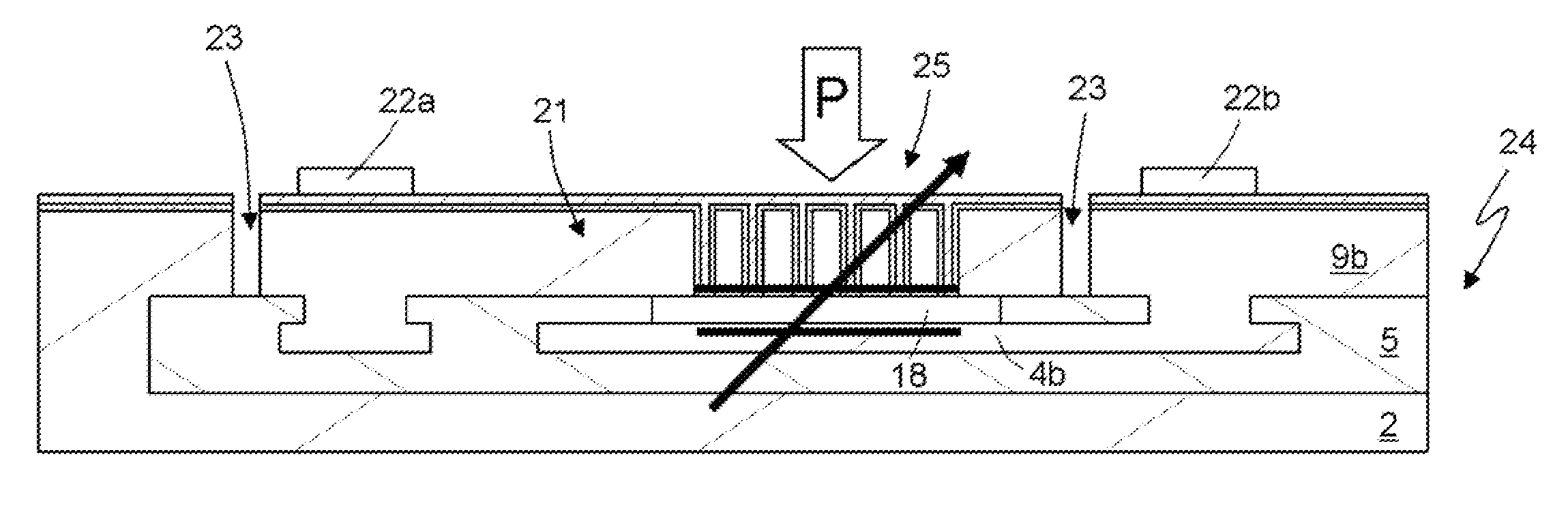
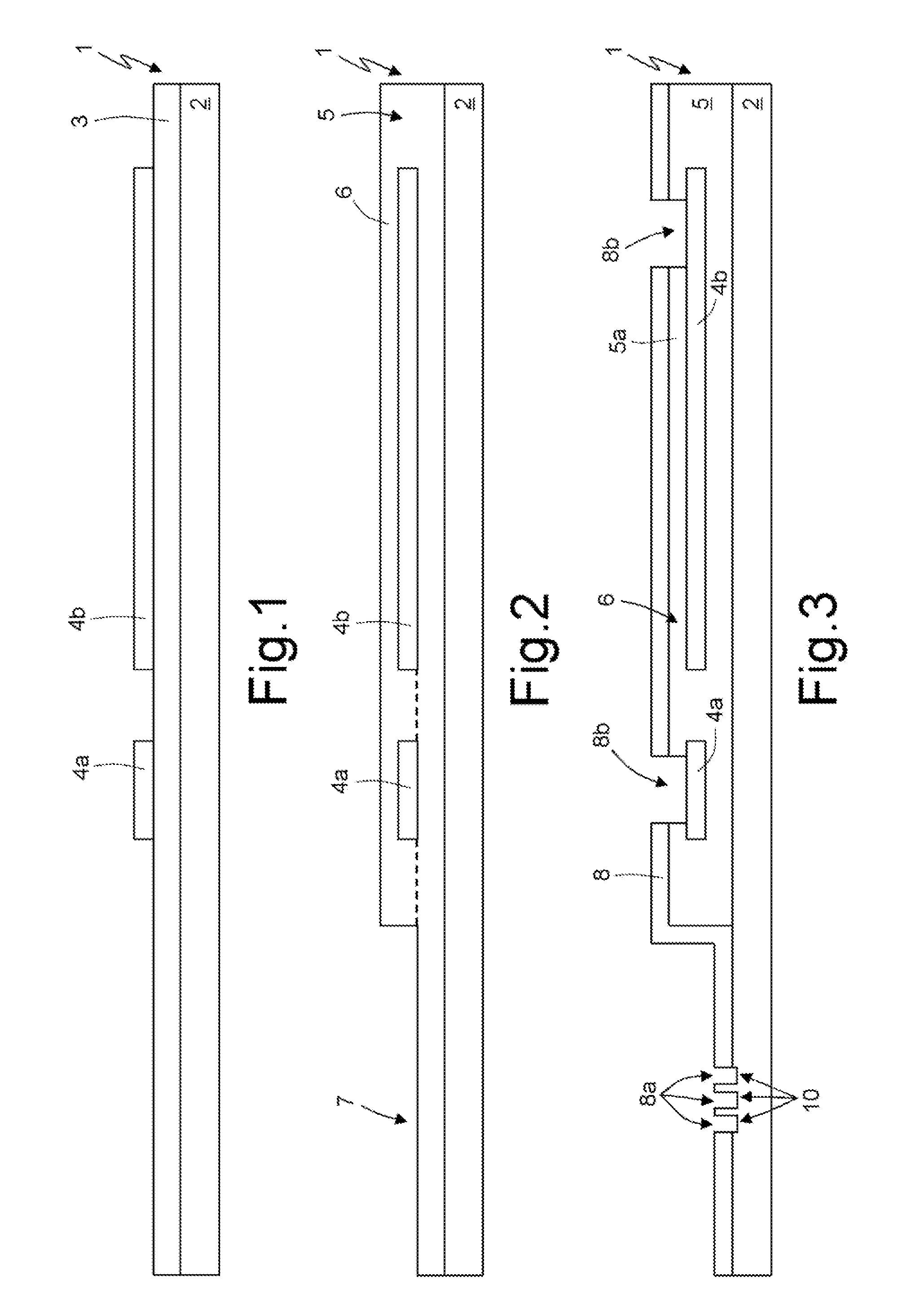
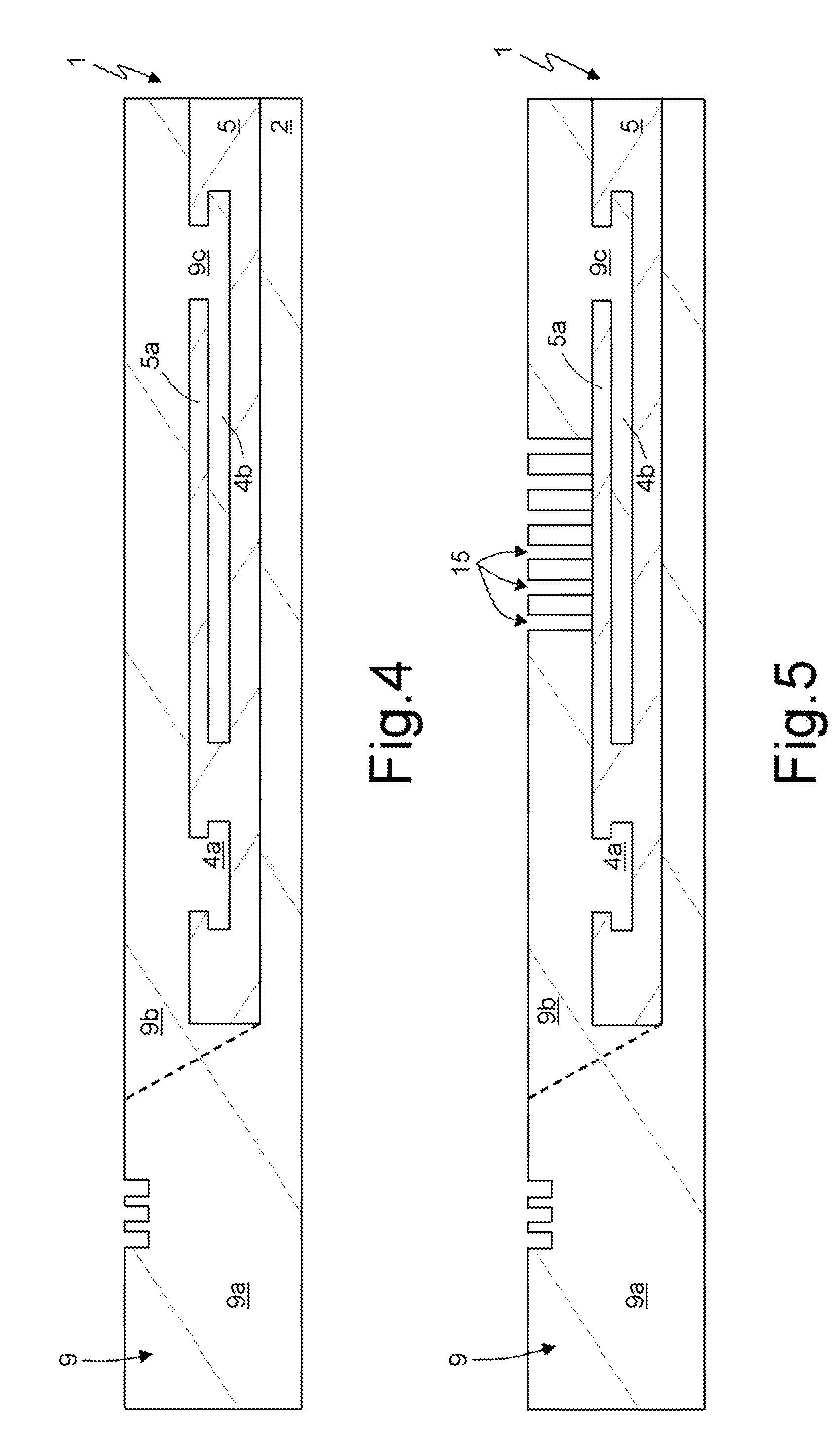
BACKGROUND[0001]1. Technical Field[0002]The present disclosure relates to a process for manufacturing MEMS devices. In particular, the disclosure relates to the manufacture of devices having a membrane suspended above buried cavities or channels.[0003]2. Description of the Related Art[0004]Hereinafter, reference will be made to the manufacture of a capacitive pressure sensor having a suspended region, also referred to as membrane, that is able to move with respect to the rest of the structure.[0005]The disclosure is not, however, limited to this sensor, but applies also to other MEMS sensors, actuators and devices having buried channels, for instance for the use in microfluidic devices.[0006]In particular, in the case of pressure sensors of a capacitive type, the membrane represents a variable electrode, facing a fixed portion forming a fixed electrode and separated from the latter by a buried cavity.[0007]Various techniques are known for manufacturing the membrane, based upon gluin...

Claims


Application Information

Patent Timeline
IPC IPC(8): H01L29/84H01L21/02
CPCB81B2201/0264B81B2203/0109B81C2201/0109B81C1/00047B81C1/00476B81B2203/0127
Inventor CORONA, PIETROLOSA, STEFANOGELMI, ILARIACAMPEDELLI, ROBERTO
Owner STMICROELECTRONICS SRL
Why Eureka
Try Eureka