Integrated circuit packaging system with package-on-package and method of manufacture thereof

a technology of integrated circuit and packaging system, which is applied in the direction of electrical apparatus, semiconductor devices, semiconductor/solid-state device details, etc., can solve the problems of long time-consuming and laborious, and the solution to these problems has eluded those skilled in the ar

Active Publication Date: 2011-02-17
STATS CHIPPAC LTD
View PDF15 Cites 73 Cited by
  • Summary
  • Abstract
  • Description
  • Claims
  • Application Information

AI Technical Summary

Problems solved by technology

While these approaches provide more functions within an integrated circuit, they do not fully address the requirements for integration, performance, and cost reduction.
Solutions to these problems have been long sought but prior developments have not taught or suggested any solutions and, thus, solutions to these problems have long eluded those skilled in the art.

Method used


Image

  • Integrated circuit packaging system with package-on-package and method of manufacture thereof
  • Integrated circuit packaging system with package-on-package and method of manufacture thereof
  • Integrated circuit packaging system with package-on-package and method of manufacture thereof

Examples


first embodiment

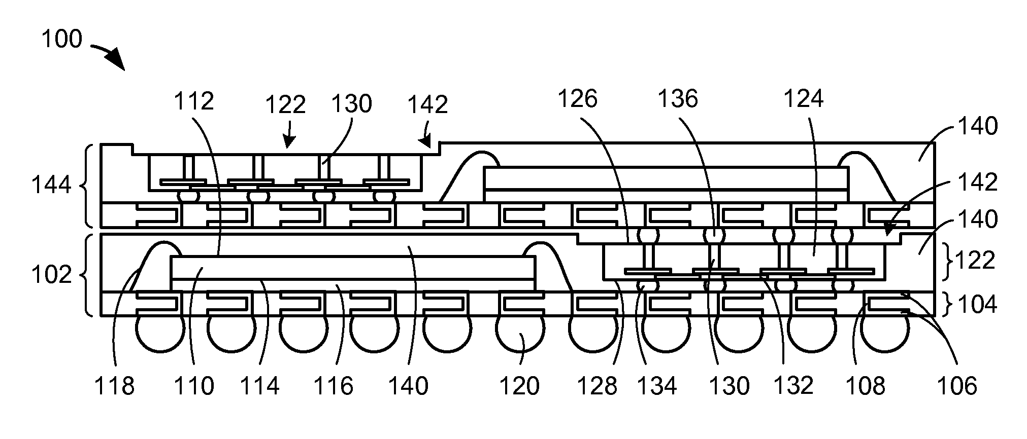
[0022]Referring now to FIG. 1, therein is shown a cross-sectional view of an integrated circuit packaging system 100 along a section line 1-1 of FIG. 2 in the present invention. The integrated circuit packaging system 100 can include a base integrated circuit package 102.

[0023]The base integrated circuit package 102 can include a substrate 104, such as a printed circuit board (PCB), a laminated plastic substrate, a laminated ceramic substrate, or a carrier. The substrate 104 can include a substrate pad 106, such as a contact pad, a bond pad, or a bump pad, and a substrate via 108, such as a hole filled with a conductive material. The substrate pad 106 and the substrate via 108 can be connected for providing an electrical interconnection between a top surface and a bottom surface of the substrate 104.

[0024]The base integrated circuit package 102 can include a component 110, such as an integrated circuit, a die, a flip chip, or a chip having a redistribution layer (RDL). The component...

second embodiment

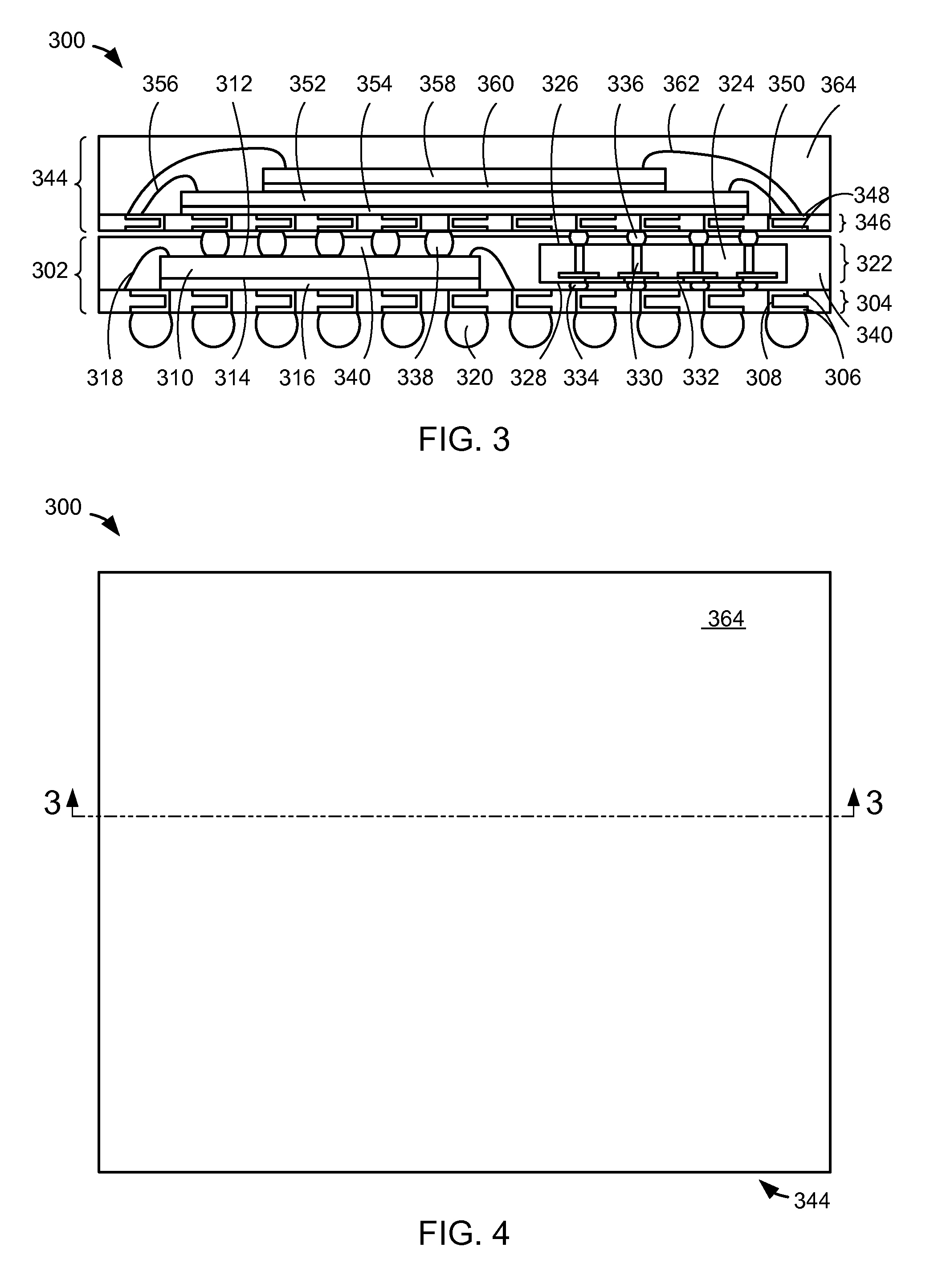
[0046]Referring now to FIG. 3, therein is shown a cross-sectional view of an integrated circuit packaging system 300 along a section line 3-3 of FIG. 4 in the present invention. The integrated circuit packaging system 300 can include a base integrated circuit package 302.

[0047]The base integrated circuit package 302 can include a substrate 304, such as a printed circuit board (PCB), a laminated plastic substrate, a laminated ceramic substrate, or a carrier. The substrate 304 can include a substrate pad 306, such as a contact pad, a bond pad, or a bump pad, and a substrate via 308, such as a hole filled with a conductive material. The substrate pad 306 and the substrate via 308 can be connected for providing an electrical interconnection between a top surface and a bottom surface of the substrate 304.

[0048]The base integrated circuit package 302 can include a component 310, such as an integrated circuit, a die, a flip chip, or a chip having a redistribution layer (RDL). The component...

third embodiment

[0072]Referring now to FIG. 5, therein is shown a cross-sectional view of an integrated circuit packaging system 500 along a section line 5-5 of FIG. 6 in the present invention. The integrated circuit packaging system 500 can include a base integrated circuit package 502.

[0073]The base integrated circuit package 502 can include a substrate 504, such as a printed circuit board (PCB), a laminated plastic substrate, a laminated ceramic substrate, or a carrier. The substrate 504 can include a substrate pad 506, such as a contact pad, a bond pad, or a bump pad, and a substrate via 508, such as a hole filled with a conductive material. The substrate pad 506 and the substrate via 508 can be connected for providing an electrical interconnection between a top surface and a bottom surface of the substrate 504.

[0074]The base integrated circuit package 502 can include a component 510, such as an integrated circuit, a die, a flip chip, or a chip having a redistribution layer (RDL). The component...


PUM


Abstract

A method of manufacture of an integrated circuit packaging system includes: providing a substrate; mounting a component over a side of the substrate; forming an interface module having a module via in any location for connectivity to the substrate; and mounting the entirety of the interface module over a portion of the side of the substrate next to the component.

Description

TECHNICAL FIELD[0001]The present invention relates generally to an integrated circuit packaging system, and more particularly to a system for an integrated circuit packaging system with package-on-package.BACKGROUND ART[0002]Consumer electronics requirements demand more integrated circuits in an integrated circuit package while paradoxically providing less physical space in the system for the increased integrated circuits content. Continuous cost reduction is another requirement. Some technologies primarily focus on integrating more functions into each integrated circuit. Other technologies focus on stacking these integrated circuits into a single package. While these approaches provide more functions within an integrated circuit, they do not fully address the requirements for integration, performance, and cost reduction.[0003]These increasing requirements for miniaturization are particularly noteworthy, for example, in portable information and communication devices such as cellular...

Claims


Application Information

Patent Timeline
Patent Type & Authority Applications(United States)
IPC IPC(8): H01L23/52H01L21/50
CPCH01L23/3128H01L23/49827H01L2924/30107H01L2924/10253H01L2224/32145H01L2224/16145H01L2225/1058H01L2225/1023H01L2225/1088H01L2924/3511H01L2924/1815H01L2224/48227H01L2224/32225H01L24/48H01L2924/18161H01L2924/15311H01L2225/06568H01L2224/73265H01L23/49833H01L25/0655H01L25/105H01L25/50H01L2224/16225H01L2224/48225H01L2224/73207H01L2924/00012H01L2924/00H01L24/73H01L2224/45014H01L2924/00014H01L2924/14H01L2924/181H01L2224/45015H01L2924/207H01L2924/206
Inventor SHIN, HANGILYANG, DEOKKYUNGHA, JONG-WOO
Owner STATS CHIPPAC LTD
Why Eureka
Try Eureka