Display Device

a display device and liquid crystal display technology, applied in static indicating devices, non-linear optics, instruments, etc., can solve the problem of unavoidable low transmittance of the whole liquid crystal display, and achieve the effect of less flicker and high transmittan

Active Publication Date: 2011-02-24
INNOLUX CORP
View PDF9 Cites 0 Cited by
  • Summary
  • Abstract
  • Description
  • Claims
  • Application Information

AI Technical Summary

Benefits of technology

[0010]According to the present invention, a display device with high transmittance, less flicker is provided.
[0012]Furthermore, the top substrate is positioned on a top side of the display device. A common electrode is formed on an under surface of the top substrate. A liquid crystal layer is sandwiched by the top electrode and the common electrode, wherein the top electrode is employed as a pixel electrode of the display device. Significantly, the bottom electrode is also transparent and can be formed by the same material as the top electrode, such as ITO. The bottom electrode is coupled with the common electrode. Therefore, the Cst line in accordance with prior art which is not transparent can be omitted. A display device with high transmittance, less flicker can be realized.

Problems solved by technology

Accordingly, when the Cst area is enlarged to minimize the flicker phenomenon, the transmittance of the whole liquid crystal display unavoidably becomes low.

Method used


Image

  • Display Device
  • Display Device
  • Display Device

Examples


Embodiment Construction

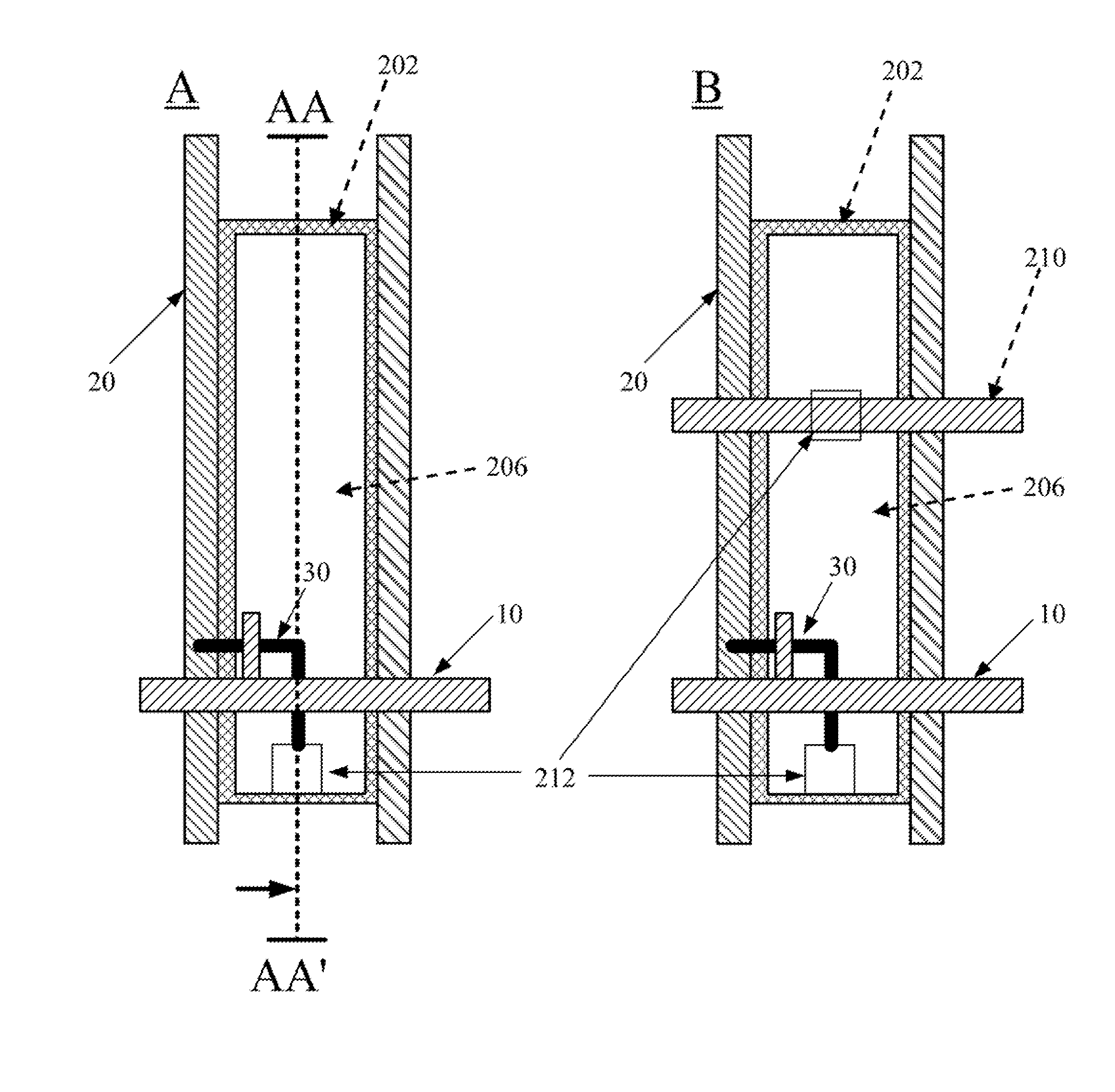
[0022]Please refer to FIG. 4, which depicts a simple structure top view diagram of pixel units A, B according to the present invention. In the following embodiments, a liquid crystal display is illustrated as a display device of the present invention. The pixel unit A of the liquid crystal display in accordance with the present invention comprises a gate line 10, a data line 20, a polysilicon layer (p-Si) 30 is patterned as an active channel region of a TFT (Thin Film Transistor), a bottom electrode 202, a top electrode 206 and at least one contact hole 212. A storage capacitance Cst 208 according to the present invention is formed by the bottom electrode 202 and the top electrode 206 (details will be introduced later). Therefore, a Cst line such as the Cst line 40 of the prior art (see FIG. 1) is not required and can be selectively omitted as shown in the pixel unit A of FIG. 4.

[0023]Alternatively, a Cst line 210 also can be formed as shown in the pixel unit B of FIG. 4 according t...


PUM


Abstract

A display device is disclosed. According to the present invention, the display device comprises a bottom substrate, a plurality of interlayers, a first passivation layer, a bottom electrode, a second passivation layer, a top electrode and a top substrate. The interlayers are formed on the bottom substrate, including a patterned polysilicon layer, a data line and a gate line disposed therein. The first passivation layer is formed on the interlayers. The bottom electrode is formed on the first passivation layer. The second passivation layer is formed to cover the bottom electrode. The top electrode is formed on the second passivation layer at a position corresponding to the bottom electrode to form a storage capacitance.

Description

CROSS REFERENCE TO RELATED APPLICATION[0001]This application claims the benefit of U.S. Provisional Patent Application Ser. No. 61 / 235,683, filed Aug. 20, 2009 and Provisional Patent Application Ser. No. 61 / 247,079, filed Sep. 30, 2009.BACKGROUND OF THE INVENTION[0002]1. Field of the Invention[0003]The present invention generally relates to a display device, and more particularly to a liquid crystal display device with high transmittance, less flicker.[0004]2. Description of Prior Art[0005]Flicker is a visual defect to an AMLCD (Active Matrix Liquid Crystal Display) which has already been led a great concern in the related industry field. Various kinds of solutions have proposed to minimize the flicker phenomenon occurring on a liquid crystal display. For example, voltage adjustment, flicker compensation circuit design, gate R-C loading degradation, Cst (storage capacitance) compensation, and etc. Among those solutions, the Cst compensation can be a major choice for the manufacturer...

Claims


Application Information

Patent Timeline
Patent Type & Authority Applications(United States)
IPC IPC(8): G09G3/36
CPCG02F1/136213
Inventor SHIBAZAKI, MINORU
Owner INNOLUX CORP
Why Eureka
Try Eureka